2 Volume Mount Devices (VMDs)
In the current generation of DICE, there have been several geometries, split into families, explored in the process of discovering a geometry that satisfies fabrication, routing, and reliability requirements.
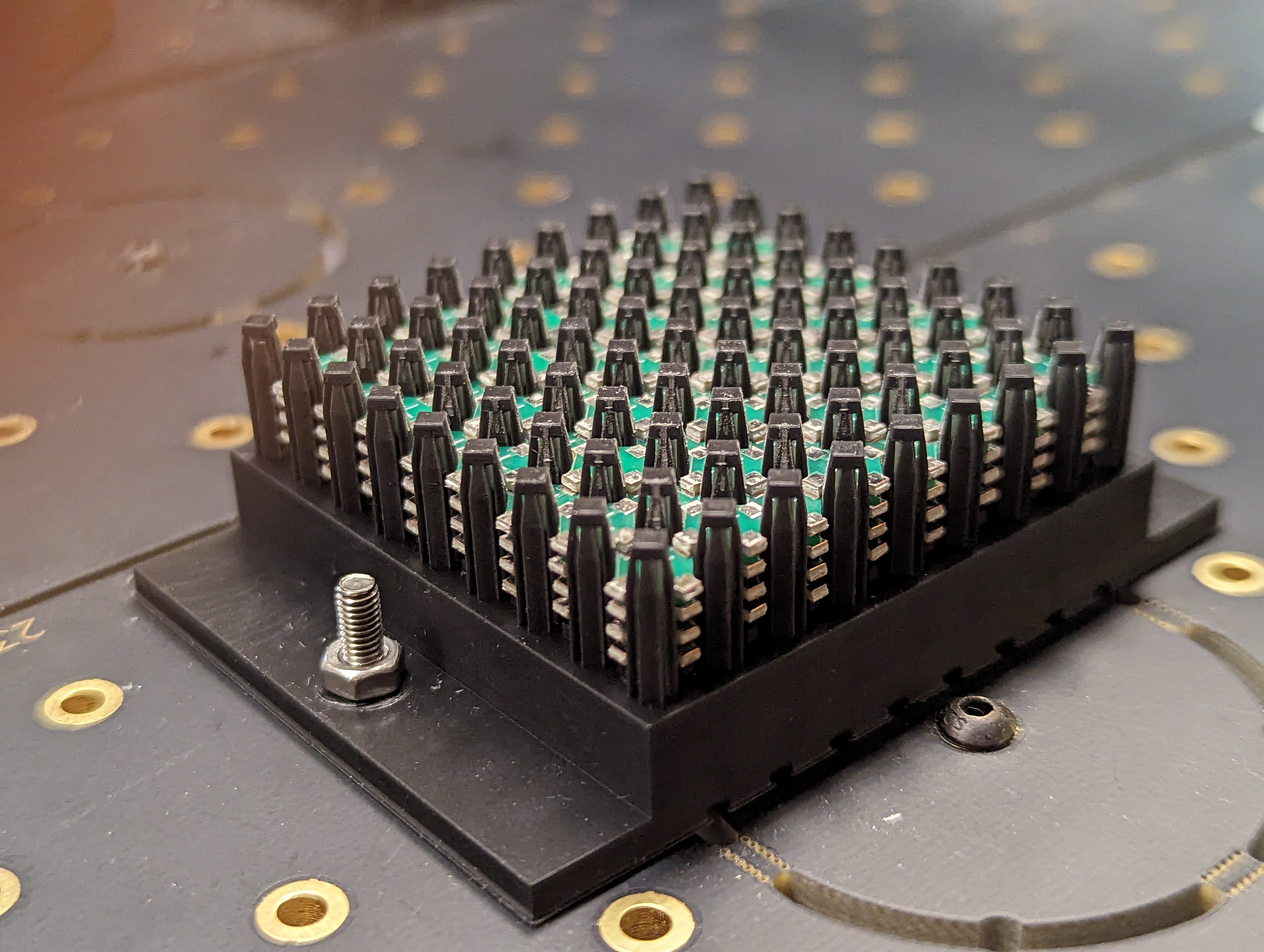
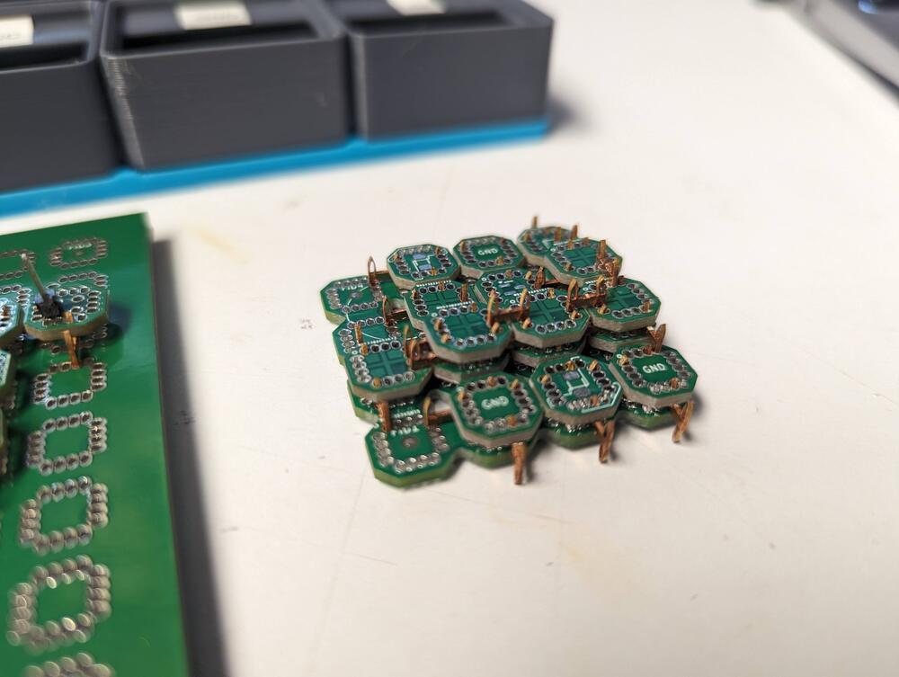
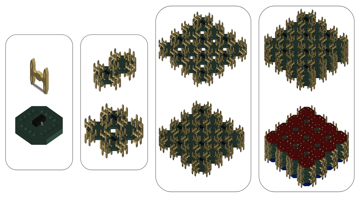
The current active geometry is 4BI, which is stacked in an alternating fashion. This geometry has been used to assemble an 8-layer, 256 tile mechanical benchmark assembly with only 2 faults that required manual intervention, significantly more elements than previous work at this abstraction level.
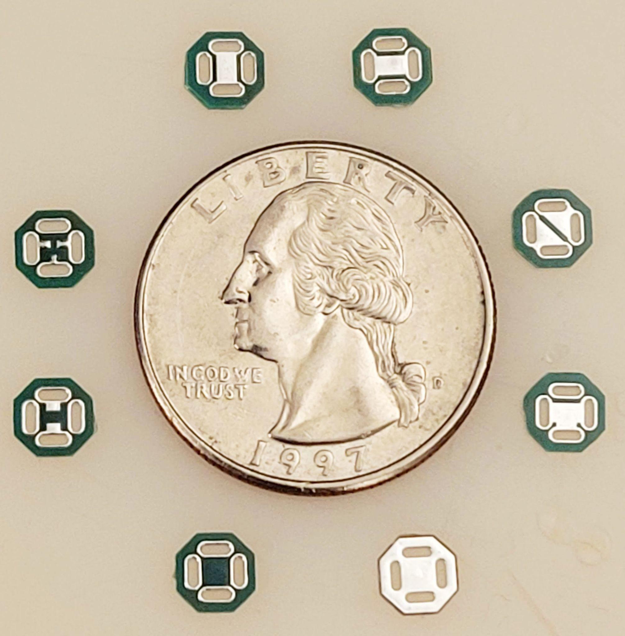
On the way to 4BI, a variety of geometry topologies and configurations were explored in the mm to cm scale (Figure 2.2).
2.1 Geometry Overview
The naming scheme is loosely based on (number of edges)(interconnect)(additional descriptors).
- number of edges: typically 4, though there have been experiments with 3-edge geometries
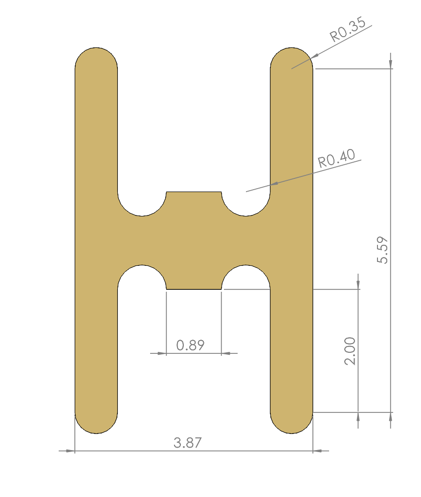
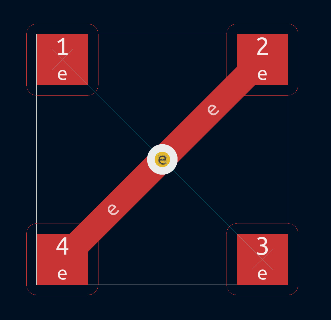
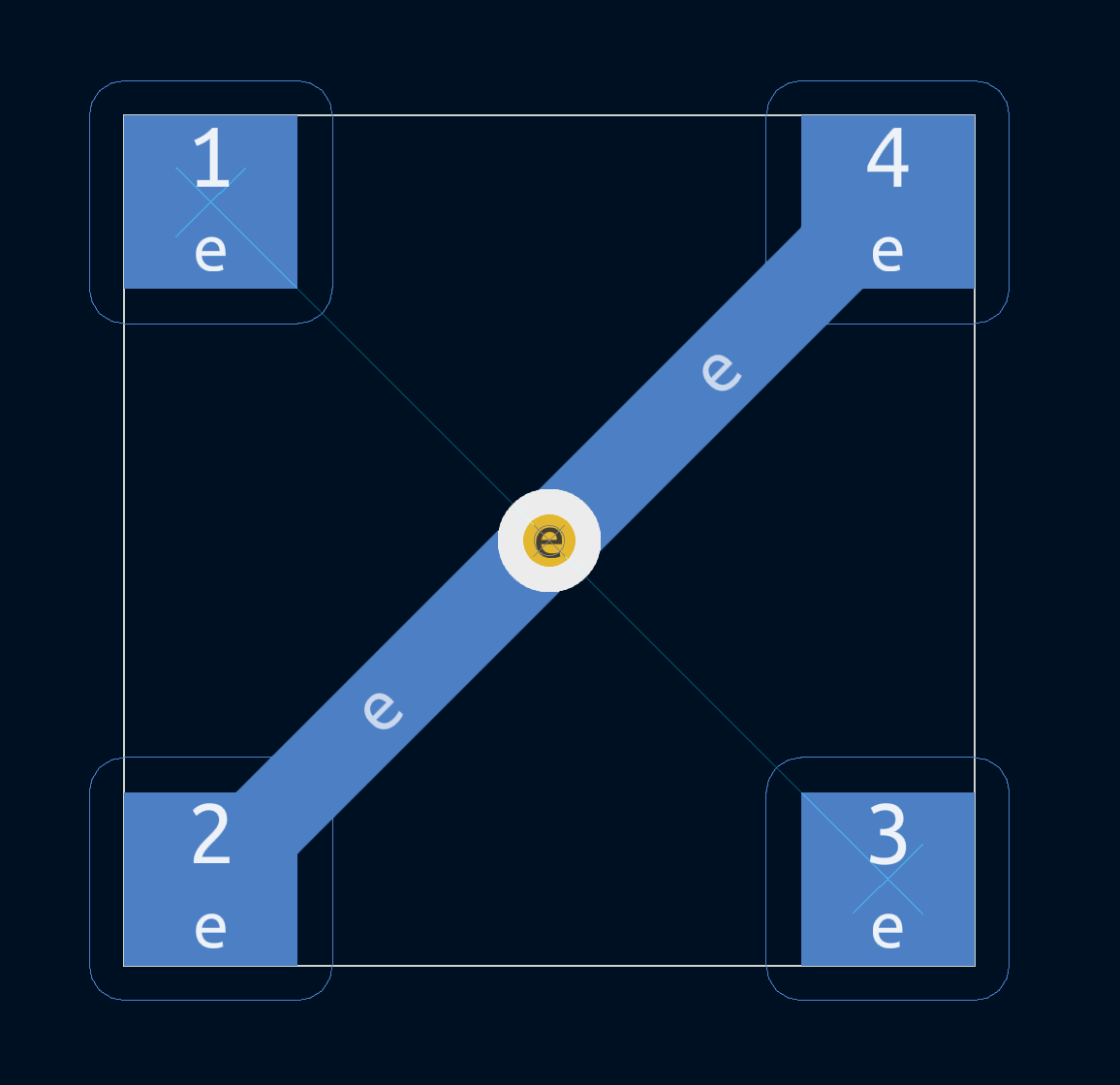
- interconnect: usually the shape of the interconnect itself; 4H refers to the H-shaped connector, 4B refers to two surface mount contacts pressed against each other, and 4BI represents surface mount contacts and alignment pillars 1
- additional descriptors: shorthand for a feature (i for integrated, p for power, k for kinematic, c for connector, 0 for just the PCB)
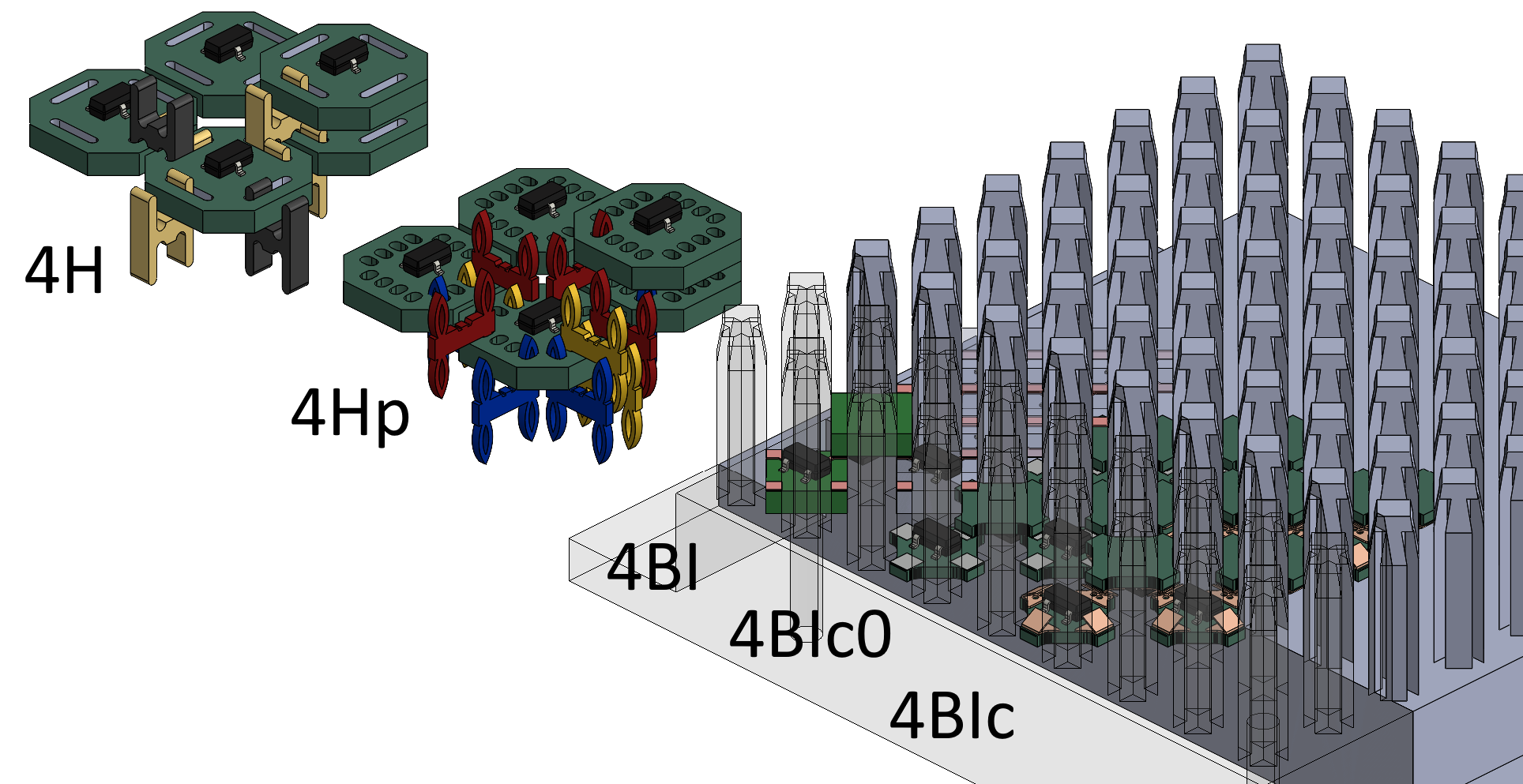
In chronological order, the naming definitions of geometries that made it to fabrication (Figure 2.3):
- 4H: 4-sided, H-shaped interconnects
- 4Hp: 4-sided, H-shaped eye-of-the-needle (H-eon) interconnects
- 4B: 4-sided, B-shaped pad-to-pad interfaces
- 4BI: 4-sided, B-shaped pad-to-pad interfaces, with I-shaped alignment pillars
- 4BIc: 4-sided, B-shaped pad-to-pad interfaces, with I-shaped alignment pillars, using compliant connector interfaces
- 4BIc0: a lite-version of 4BIc, using just the PCB. Fabricated and used in the same manner as 4BI.
| Geometry Name | 4H | 4Hp | 4B | 4BI | 4BIc0 | 4BIc |
|---|---|---|---|---|---|---|
| Connection Type | Insertion | Insertion | Pad | Pad | Pad | Pad |
| Preload Method | Local | Local | Global | Global | Global | Global |
| Element Types | 2 | 2 | 1 | 1 | 1 | 1 |
| Dedicated Power | No | Yes | No | No | No | No |
| Mech. Stability | Low | High | Low | Medium | High | High |
| Asm. Complexity | Medium | High | Low | Low | Low | Low |
| Alignment | Connector | Connector | Template | Template | Template | Template |
| Assembly Force | High | Medium | Low | Low | Low | Low |
| Joint Reliability | Poor | Good | Poor | Fair | Fair | Good |
| Scalability | Poor | Fair | Poor | Good | Good | Good |
The evolution from 4H to 4BI represented a significant shift in VMD design philosophy (Table 2.1). The 4H family utilized separate tiles and interconnects with through-hole connections requiring local preload, while the 4B family eliminated separate interconnects in favor of surface mount connections with global preload.
The big problem with the initial 4H geometry was a lack of contact compliance and interconnects with non-uniform strength properties. The 4Hp approach offered better joint reliability and uniform strength properties through a single compliant connection design but suffered from high insertion forces and complex assembly requirements.
The transition to 4B significantly simplified assembly by eliminating the separate interconnect elements altogether, but introduced alignment challenges. 4BI addressed these alignment issues through a comprehensive templating system, though at the cost of joint reliability compared to 4Hp.
This evolution demonstrated a trade-off between assembly simplicity and electrical reliability, with each geometry optimized for different aspects of the VMD concept. While 4Hp excelled at creating reliable electrical connections, 4BI proved superior for automated assembly at scale, representing the current active geometry in the VMD ecosystem.
2.2 4Hx Family
2.2.1 4H
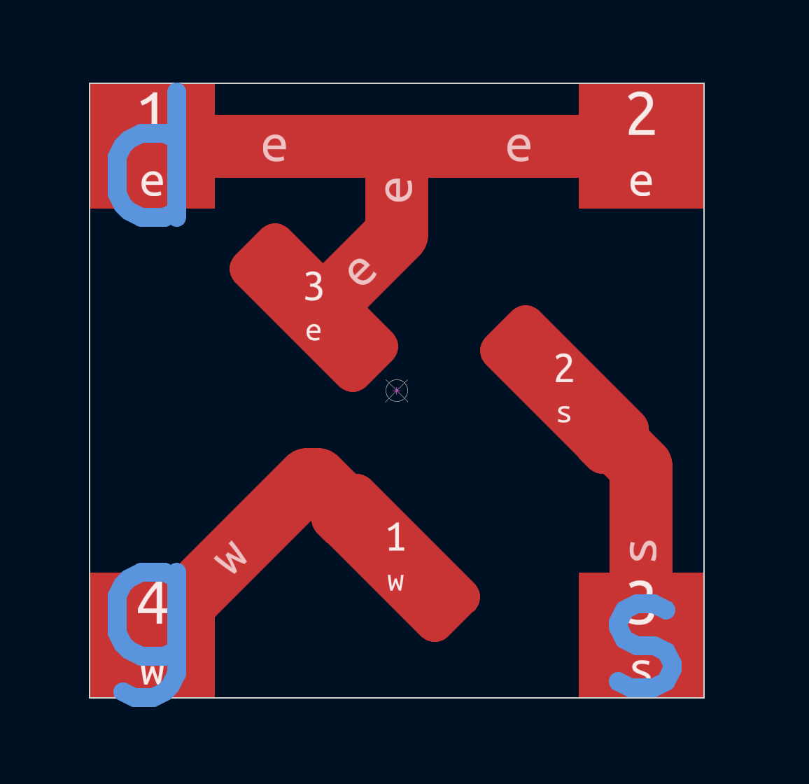
4H represents the initial foundation for the current run of DICE geometries, sometimes referred to as “O’s and H’s” (Figure 2.4). Its approach distinctly separates tiles and interconnects as fundamental elements, with tiles designed in square configurations and interconnects adopting H-shaped structures. The system employs two distinct tile categories: functional tiles containing a single component, and routing tiles facilitating net movement along a Cartesian grid.
While the 4H design benefits from conceptual simplicity, it presents several significant limitations. The provision for only a single net per edge makes ubiquitous power delivery particularly challenging; additionally, the system’s requirement for two interconnect types, conductive and insulative, resulted in inconsistent mechanical rigidity, which distorted the lattice structure and compromised assembly consistency.
The H-shaped interconnects lacked geometric compliance, causing all ports to rely solely on press-fit mechanisms and the compliance of bulk materials, which introduced unreliable forces, especially where geometric tolerances were poorly controlled; these tolerance issues proved especially difficult to manage given the large quantity of components needed and the outsourcing of designs to board houses, further complicated by designing at the boundary between reasonable size and achievable tolerance levels. An additional challenge was the single slot intended for two H’s; a single H could leave the system underconstrained and theoretically introduce assembly error.
2.2.2 4Hp
4Hp, previously named o_power, represents an iteration over the 4H design that introduced additional ports for dedicated power delivery and mechanical stability, along with compliant H interconnects (Figure 2.6). This evolution addressed several key limitations of the original 4H approach while maintaining its fundamental architecture.
The 4Hp design achieved notably improved mechanical stability, though the seating issue remained difficult to tune properly. This enhanced stability enabled consolidation to a single H-interconnect type (conductive only), resulting in more reliable mechanical behavior throughout the system. The introduction of dedicated power ports enabled ubiquitous power delivery across the grid, addressing one of 4H’s primary limitations.
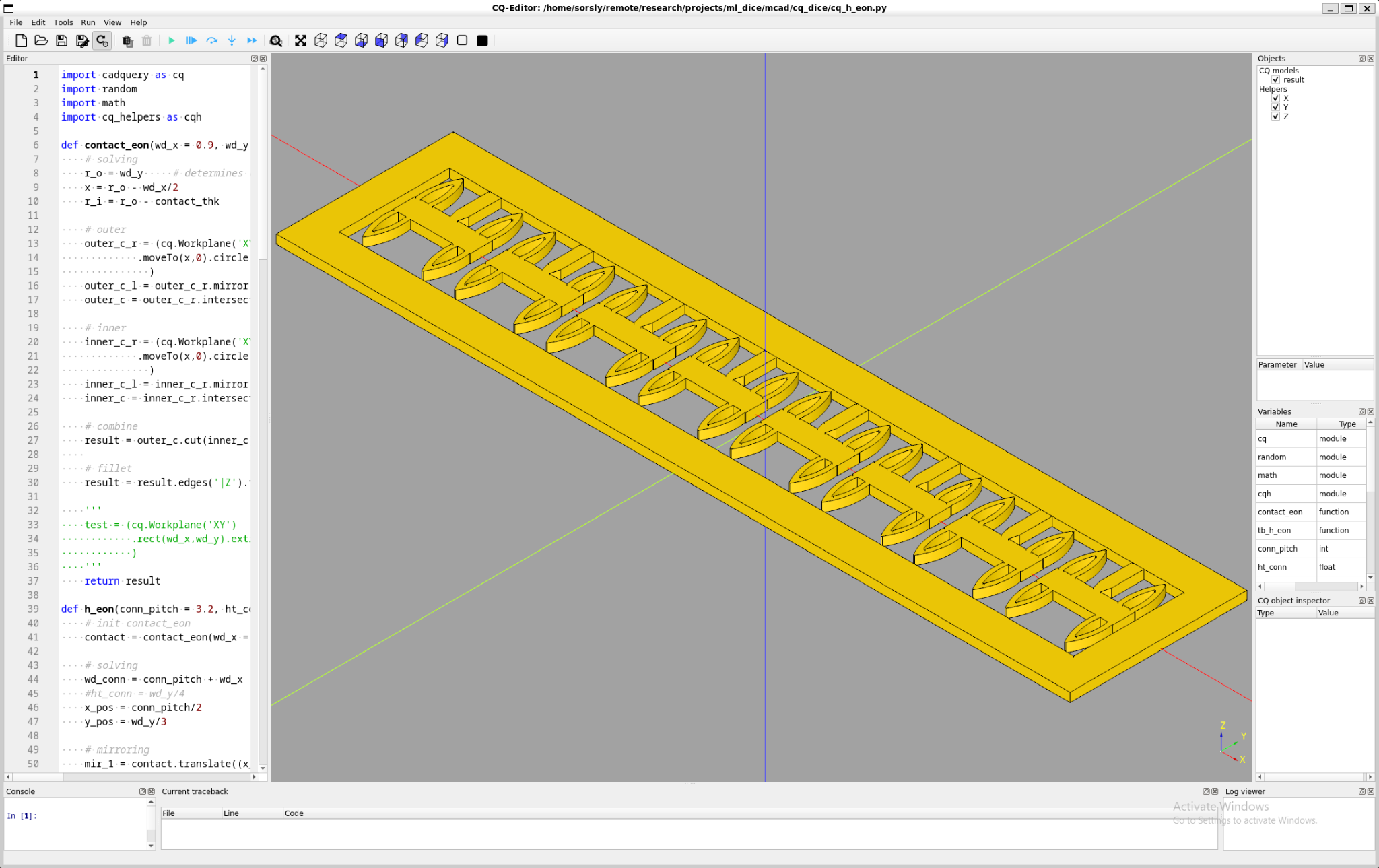
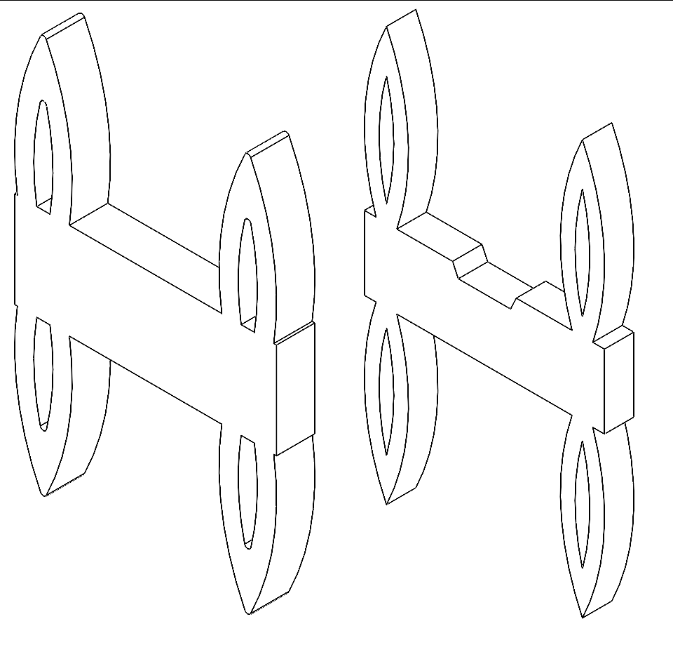
By pushing our H-connector element towards more compliant designs, we improved the reliability of each connection and increased the possible lifetime mate cycles. Eye-of-the-needle (EON) compliant designs were heavily used in the connector industry for automotive and other high performance applications. Compared to other compliant designs, EON features were easily scaled down [1]; reducing connector size with respect to tile size enabled us to move away from slots towards holes, increasing connection density on each tile. This allowed us to add dedicated power delivery connections both laterally and vertically, which also worked to improve the overall stiffness and mechanical consistency of the structure during assembly.
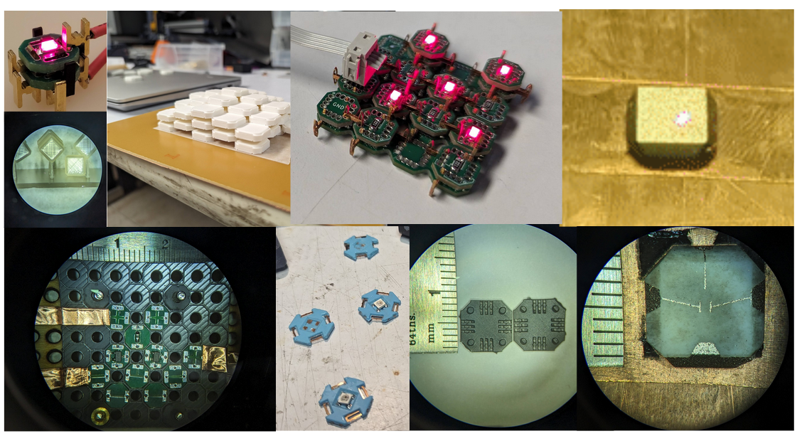
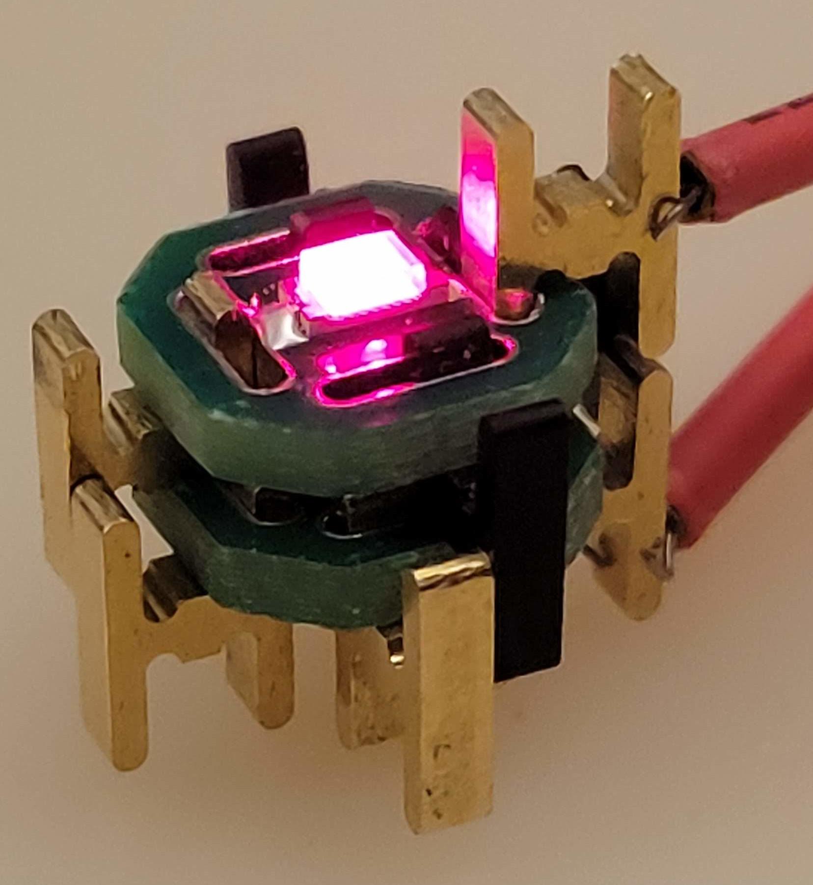
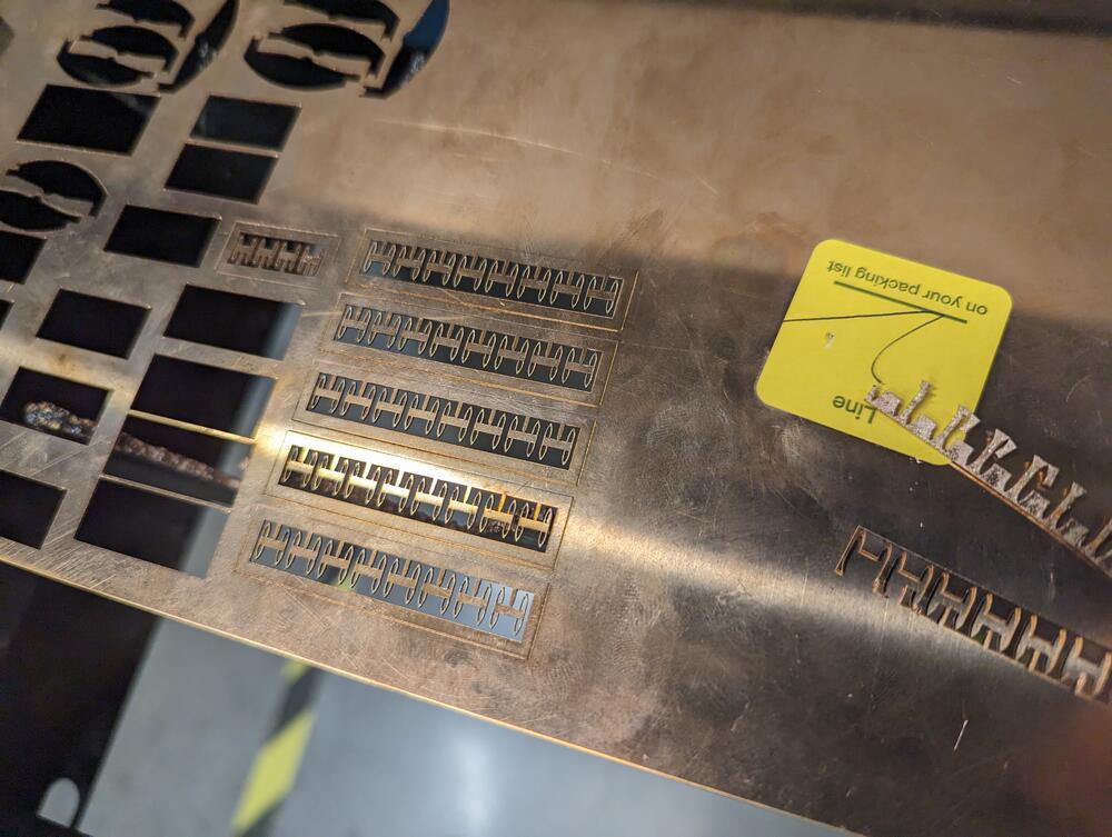
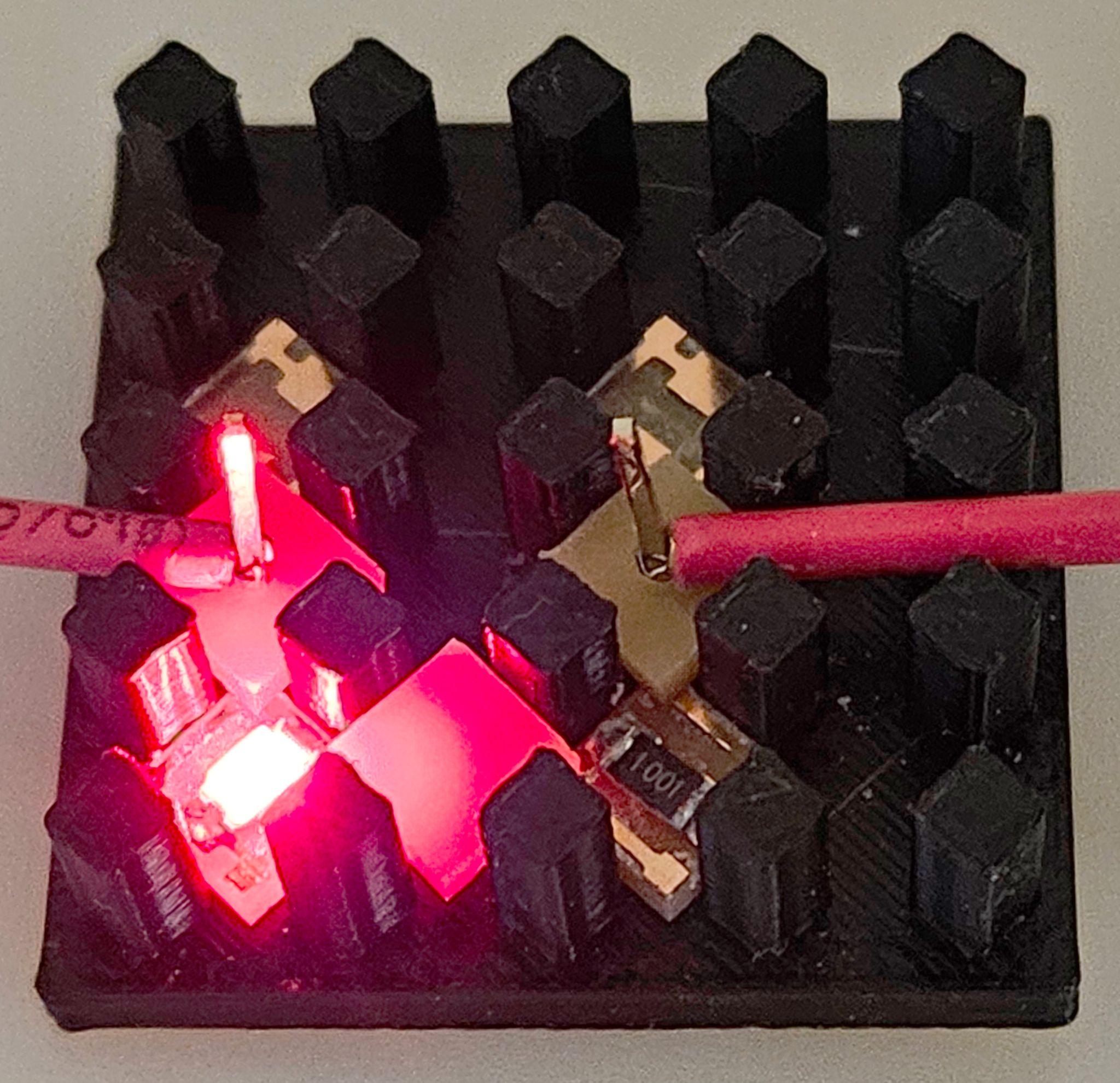
These connectors were fabricated from 0.6mm C510 Phosphor Bronze sheet stock, cut using the Fablight, a 3kW fiber laser (Figure 2.7). Initially, the H-eon connector geometry was compromised and plastically deformed after repeated cycles because the oval was cut-off; as shown in Figure 2.8 (a), I incorporated several quality-of-life design improvements such that the new geometry had a whole oval that was also above the joining strut, so the pin behaved compliantly. Additionally, the new version had an indent to set the tiebar lower into the body; the leftover stub would protrude from the design and prevent the connector from seating properly, and this feature made the connector behave in a flush manner.
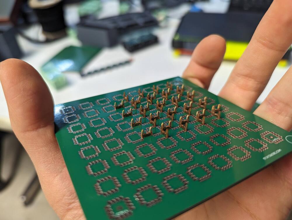
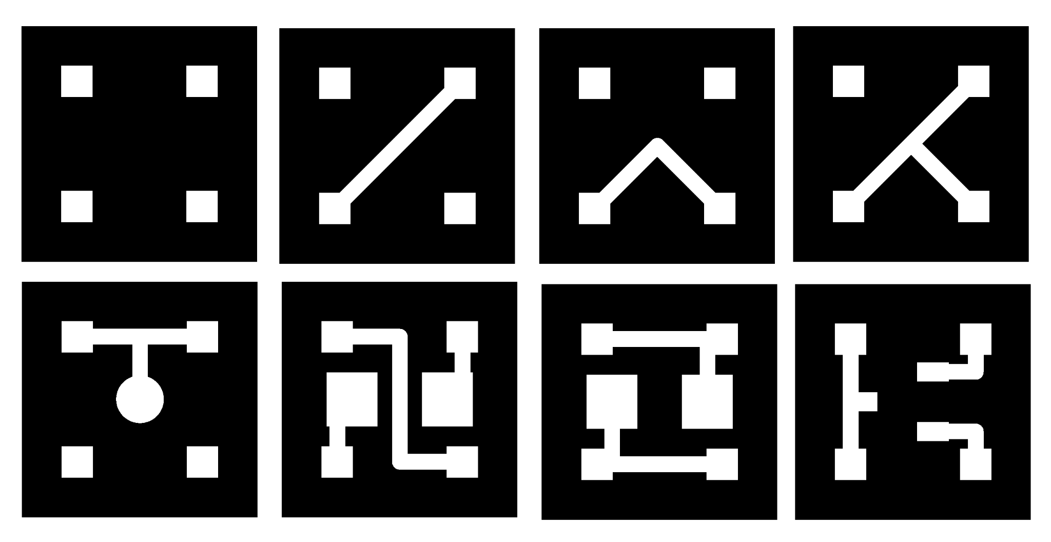
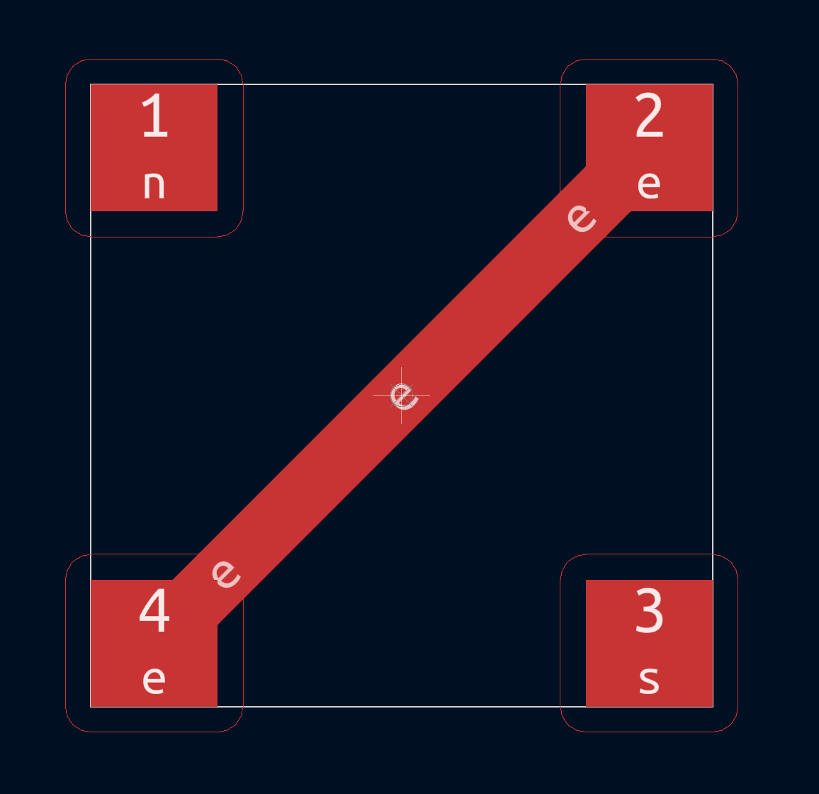
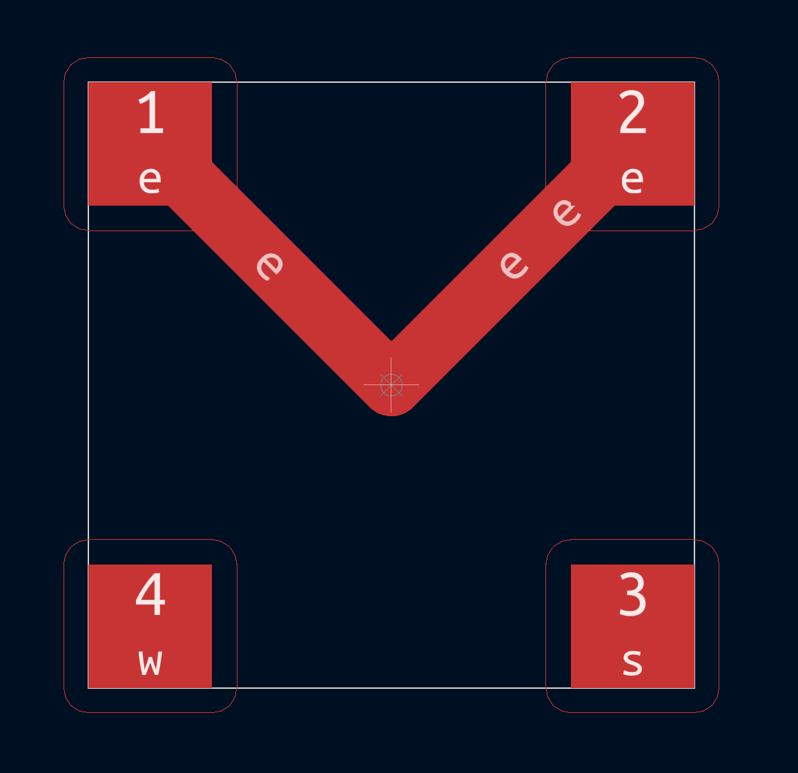
To build basic logic gates and other circuits, we developed a 6-tile library that consists of both functional tiles for components and routing tiles. As shown in Figure 2.9, routing tiles enable connecting nets to power or to selectively direct signals in different directions. This tile system maintains dedicated power ports for each side, located in such a way that structural stability is maintained while being able to selectively populate signal pins.
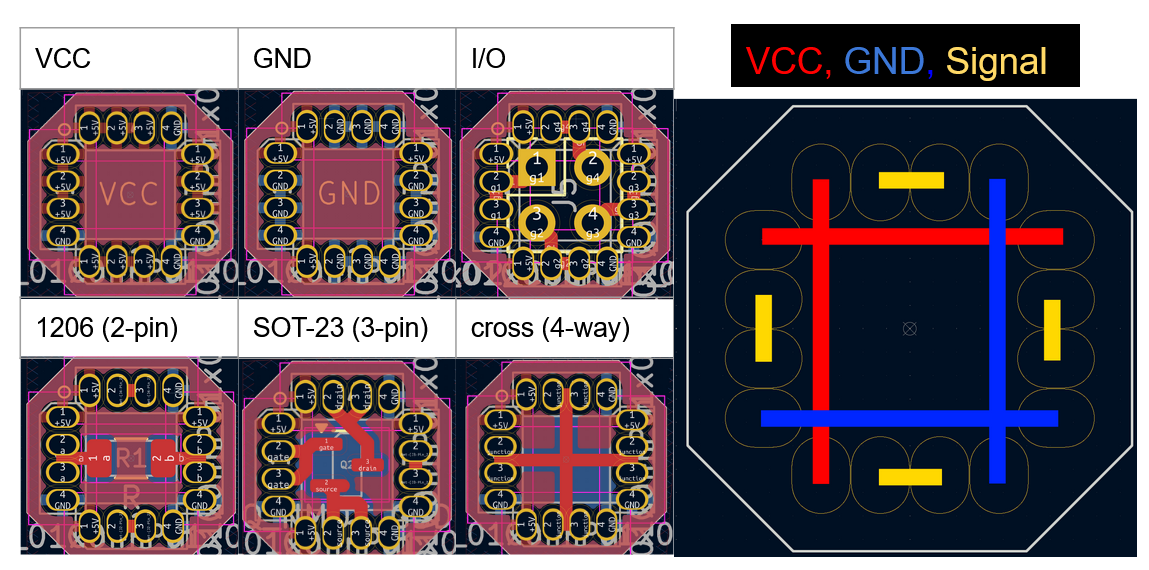
The introduction of dedicated power ports were not without cost. To avoid adding too many pins to each tile which would make it harder to shrink the design for future, higher density revisions of the geometry, a minimal number of power ports were added, which meant symmetry across the diagonal of the tile, but not axially. This meant that introducing any new tile would also necessitate adding a few variations to enable all possible routing orientations. As a result, additional tiles were introduced for easier implementation of NMOS logic, such as pull-up resistor tiles and FETs covering various degrees of freedom.


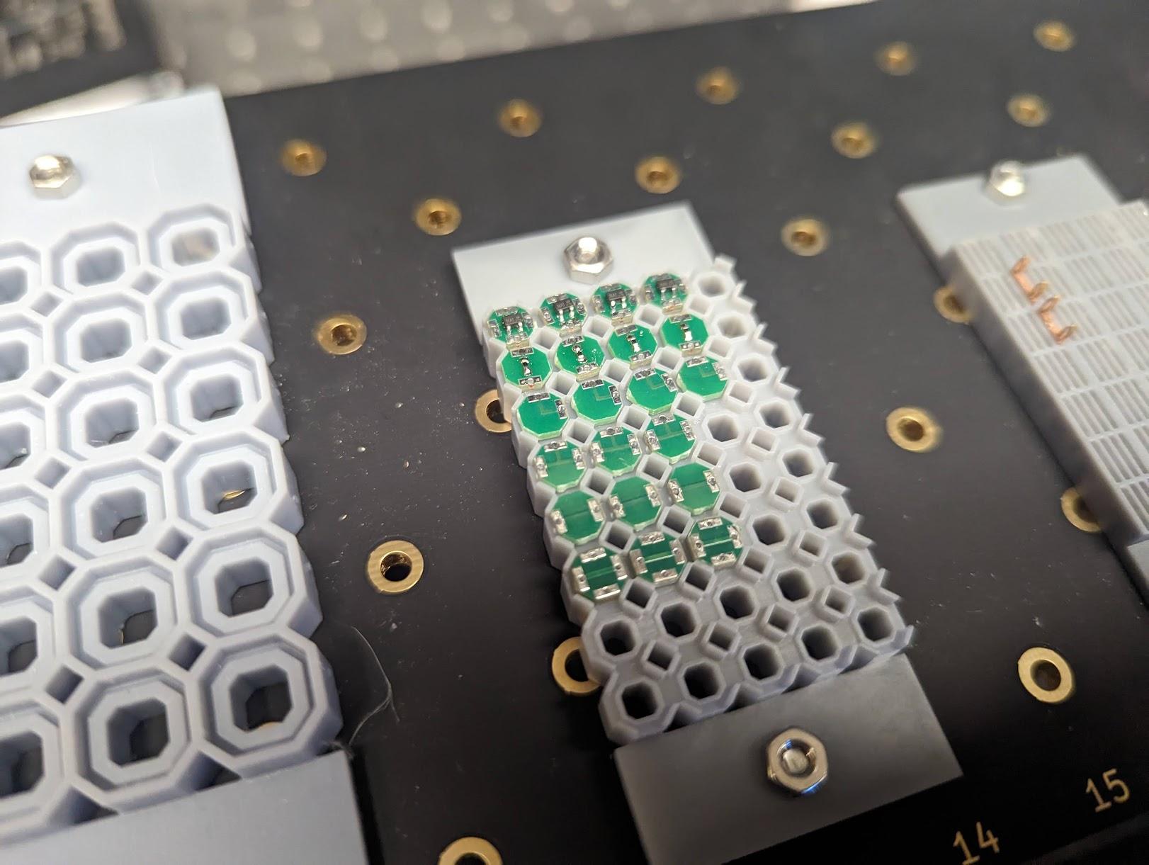
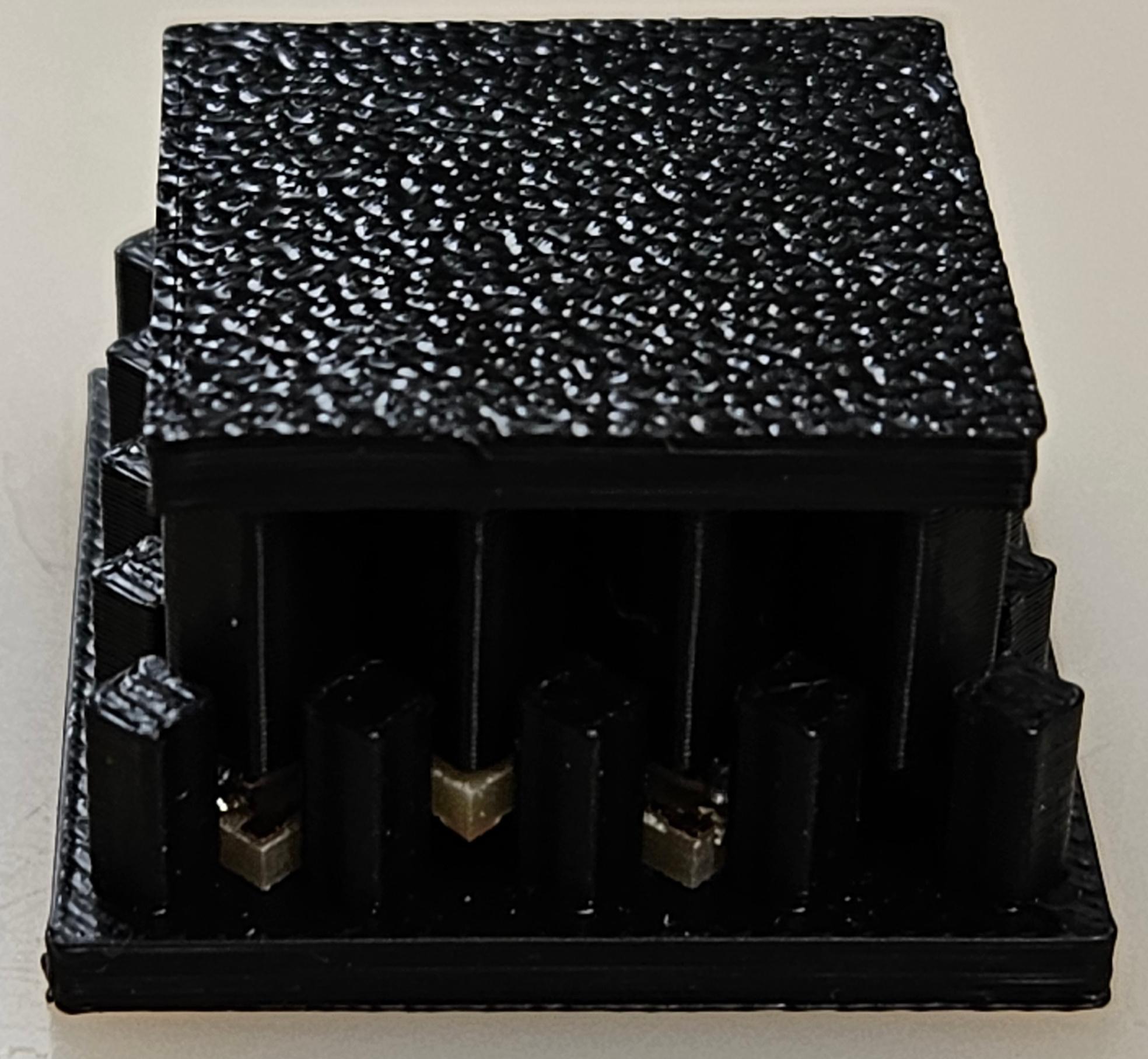
Additionally, I designed macro-tiles, which were larger tiles that were ordered in sizes of 4x4, 4x8, and 8x8, used to create sub-assemblies called “blocks”, which enable easier assembly/disassembly, or error correction, for larger structures. The structure is shown in Figure 2.11.
Despite improvements over 4H, 4Hp introduced several new challenges. The dedicated power ports led to significant assembly scale issues, with interconnect pick-and-place operations dominating assembly complexity at approximately a 4:1 ratio against tiles. The partially symmetric power ports also led to a combinatorial explosion of additional tiles to maintain design freedom, making designs more complicated and less flexible. Interconnect tolerances proved difficult to control tightly and were challenging to outsource using rapid prototyping fabrication houses. Additionally, interconnect pick-and-place operations proved less reliable than tile placement. The connection mechanism operated contrary to zero insertion force (ZIF) principles, functioning more like “much insertion force” (MIF); this high insertion force would frequently lead to component damage in common misalignment scenarios, as well as loss of stepper motor steps during assembly operations.
2.3 4Bx Family
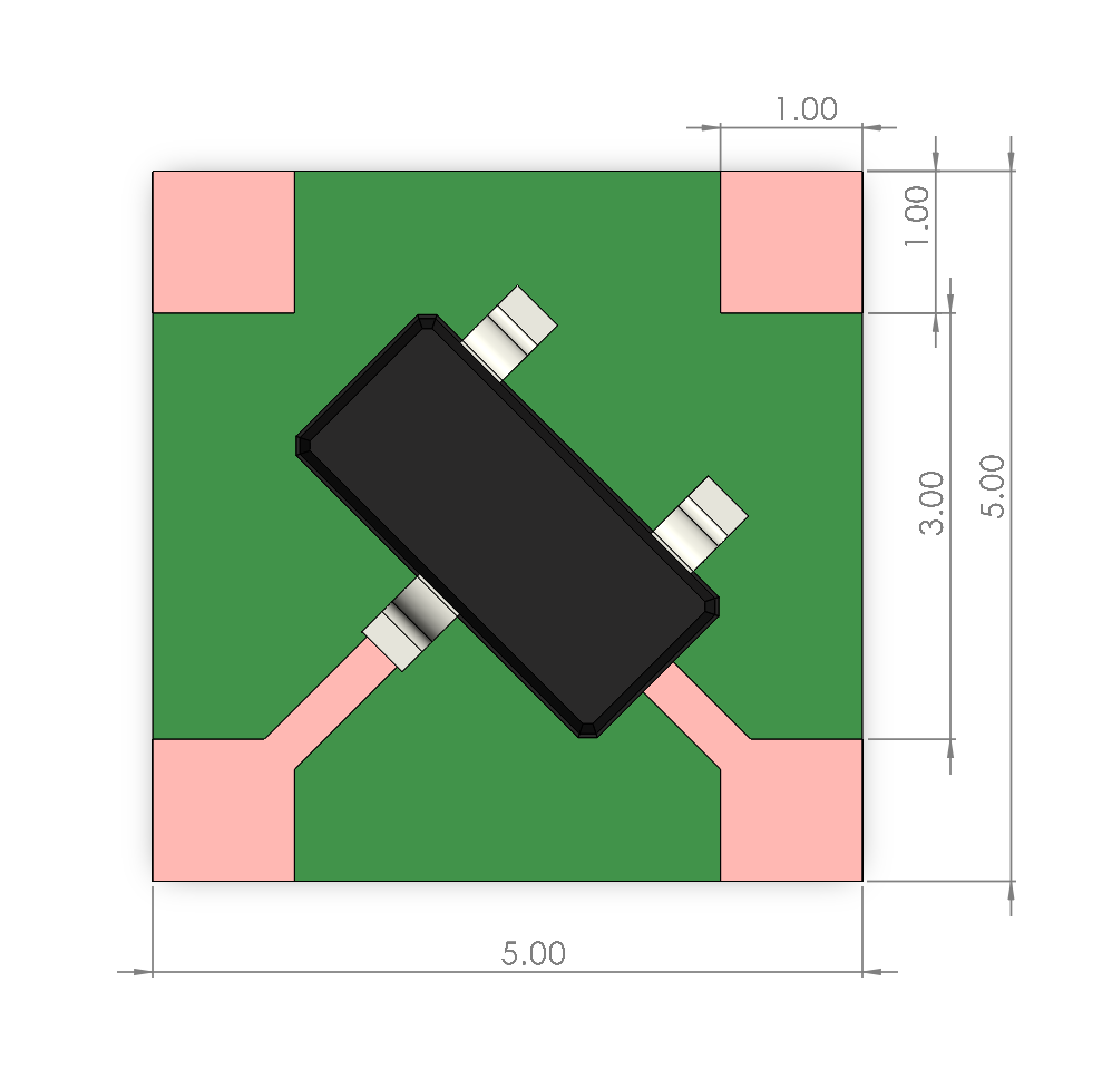
2.3.1 4B
4B represented a significant departure from the 4Hx family, eliminating the separate interconnect primitive in favor of using tiles only (Figure 2.12). This simplification offered the advantage of requiring only one end effector approach for a single primitive type, streamlining the assembly process. However, the 4B geometry introduced its own set of challenges. Since components remained on the tiles, the assembly process required either inverting the tiles or changing the end effector nozzle size to accommodate varying component dimensions. More critically, this geometry inherently lacked the templating and alignment features necessary for automated assembly, making it impossible to scale assembly without accumulating significant error.
To optimize the geometry for scaling down to smaller regimes, these new geometries were developed specifically to eliminate interconnect components. While 4B incorporated an initial alignment template, subsequent layers were left under-constrained, inevitably leading to cascading misalignment errors that compromised system integrity and reliability.
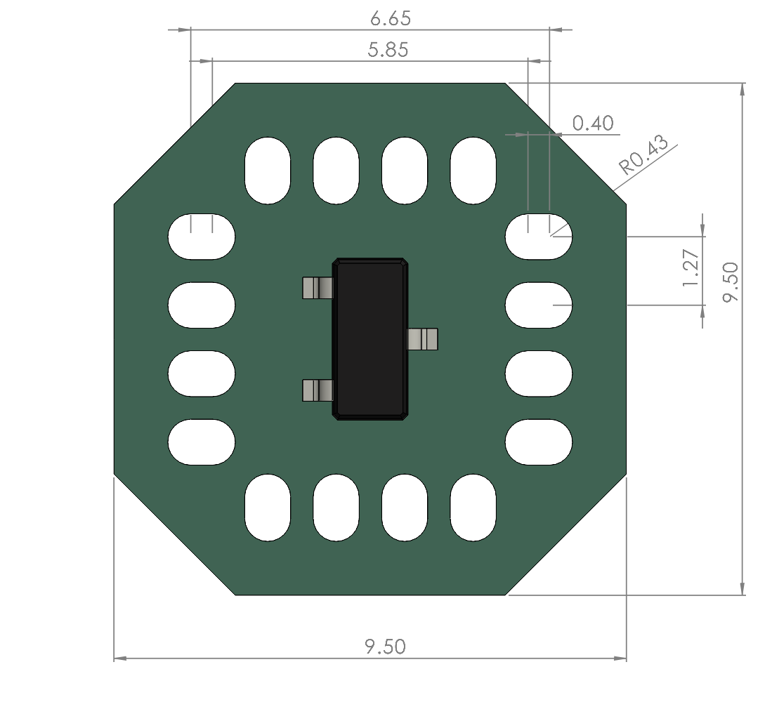
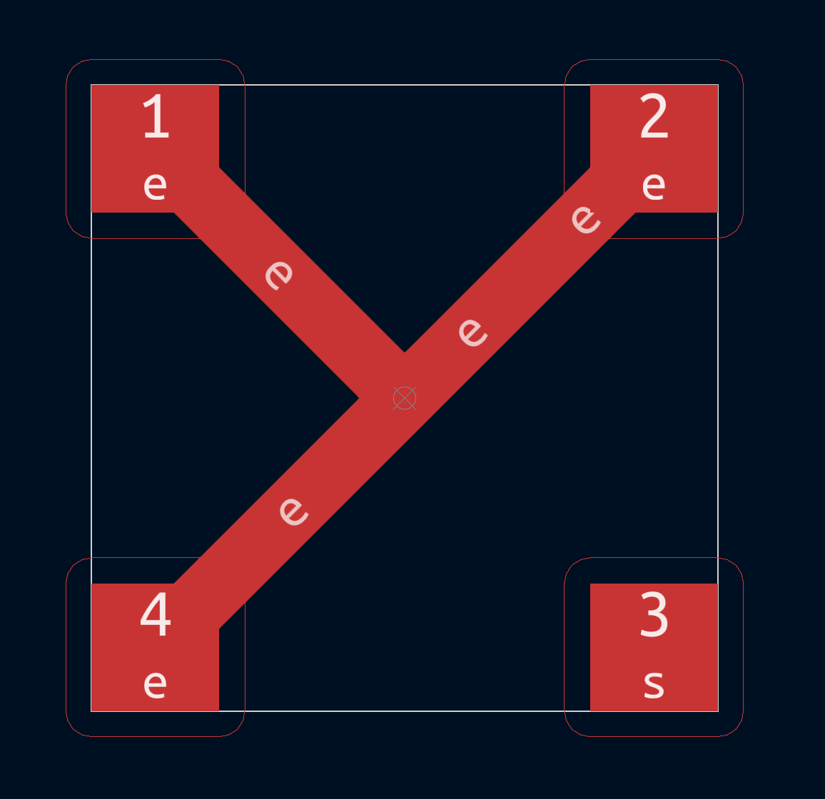
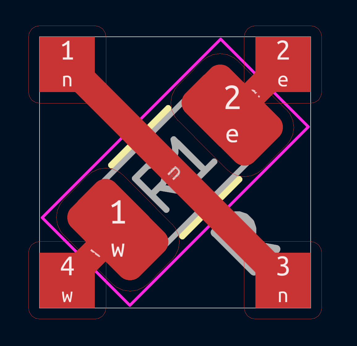
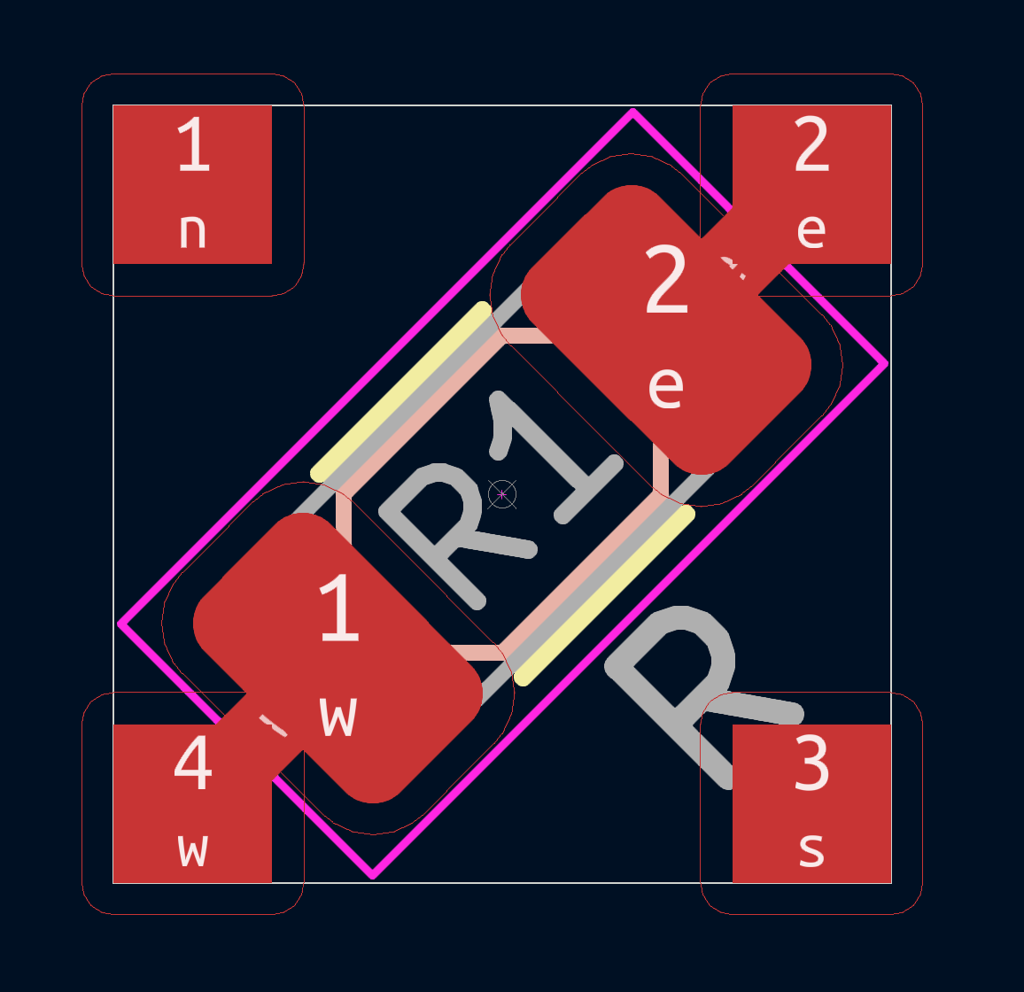
2.3.2 4BI
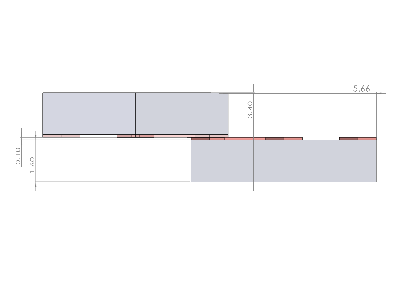
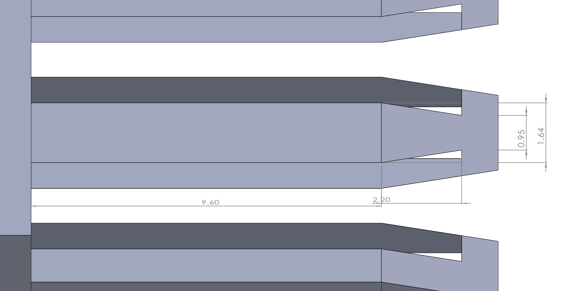
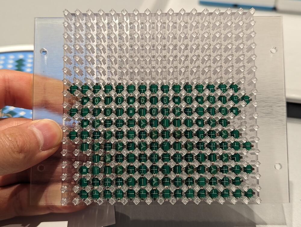
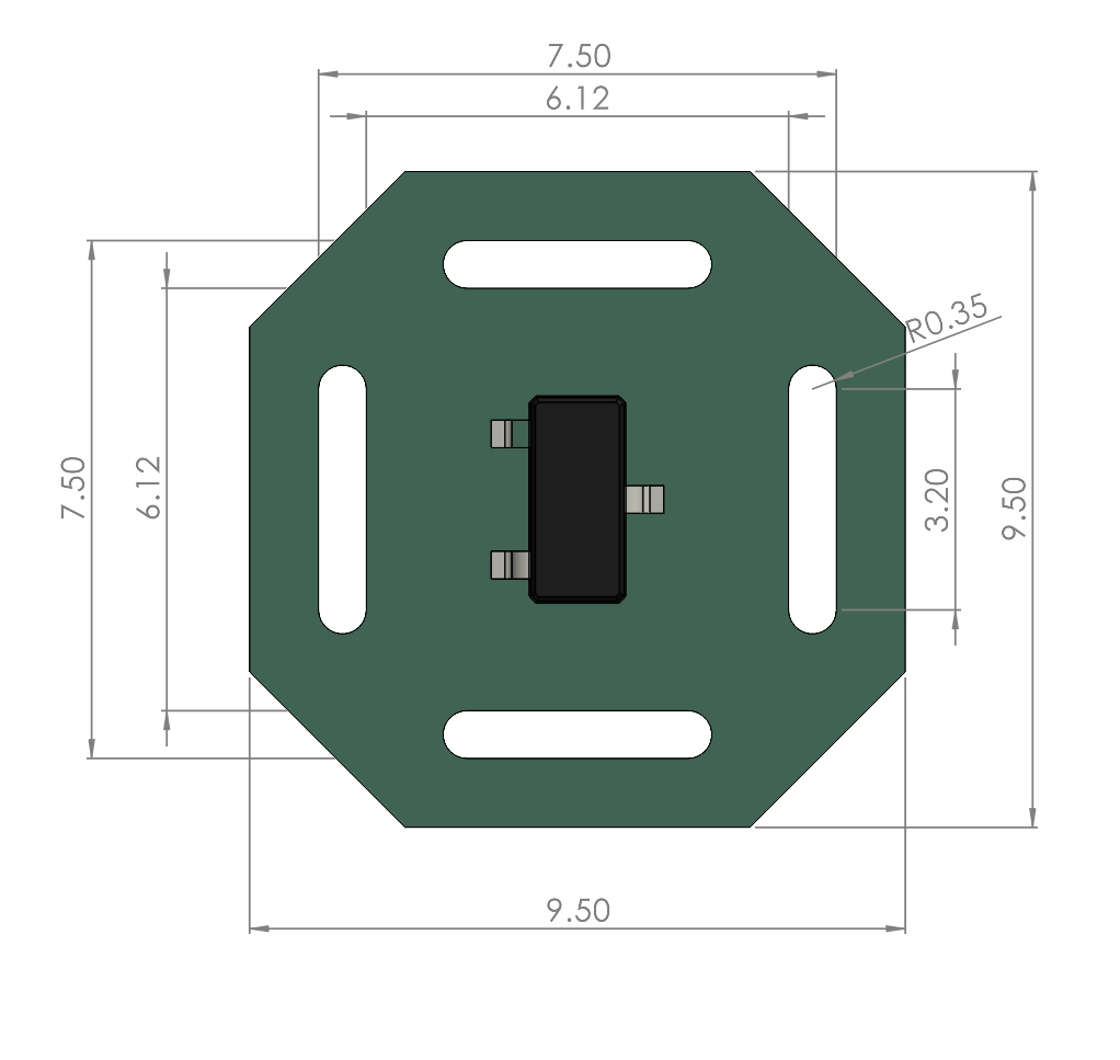
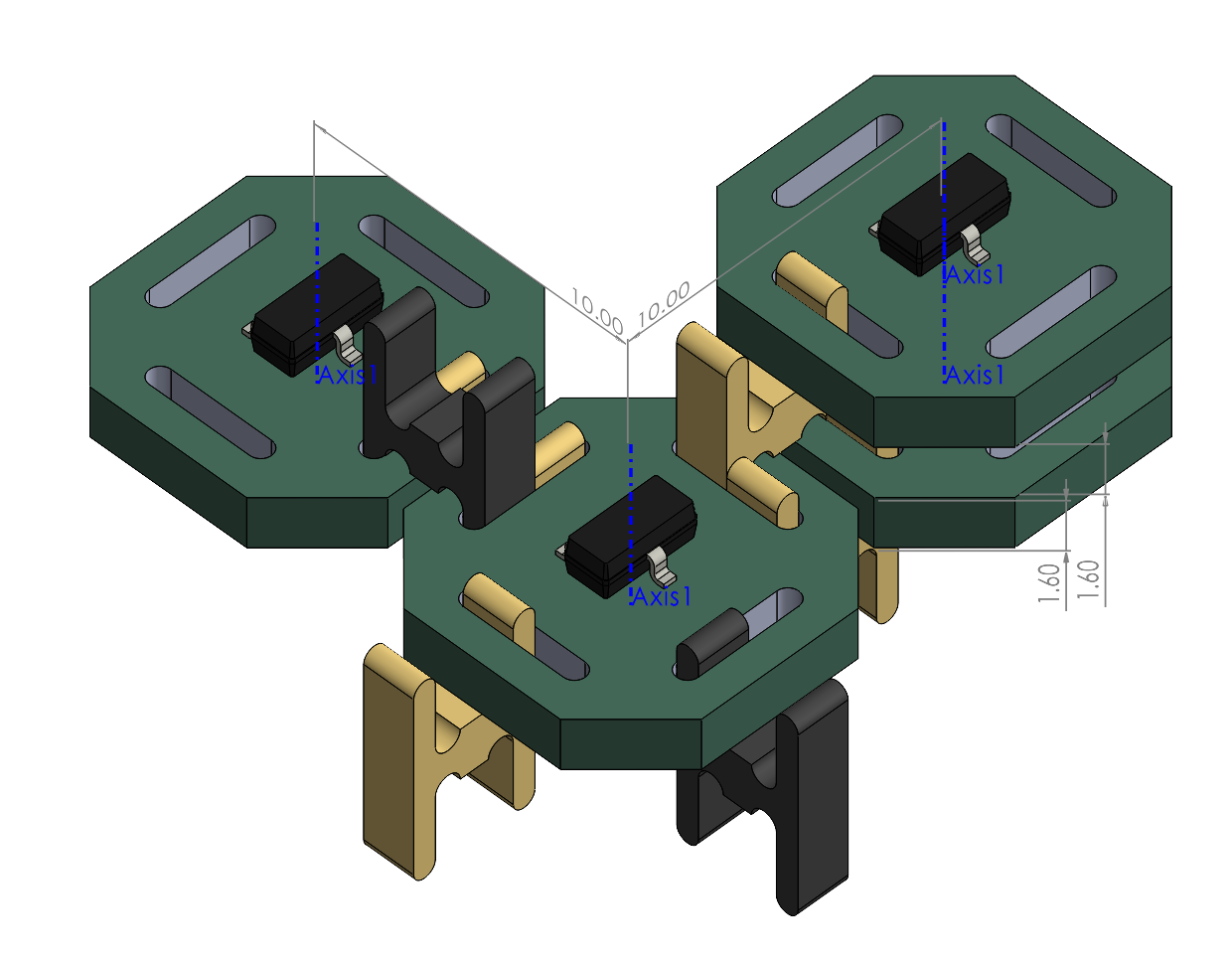
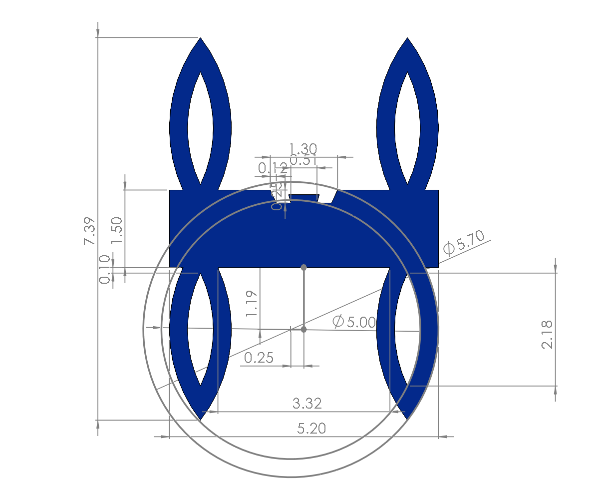
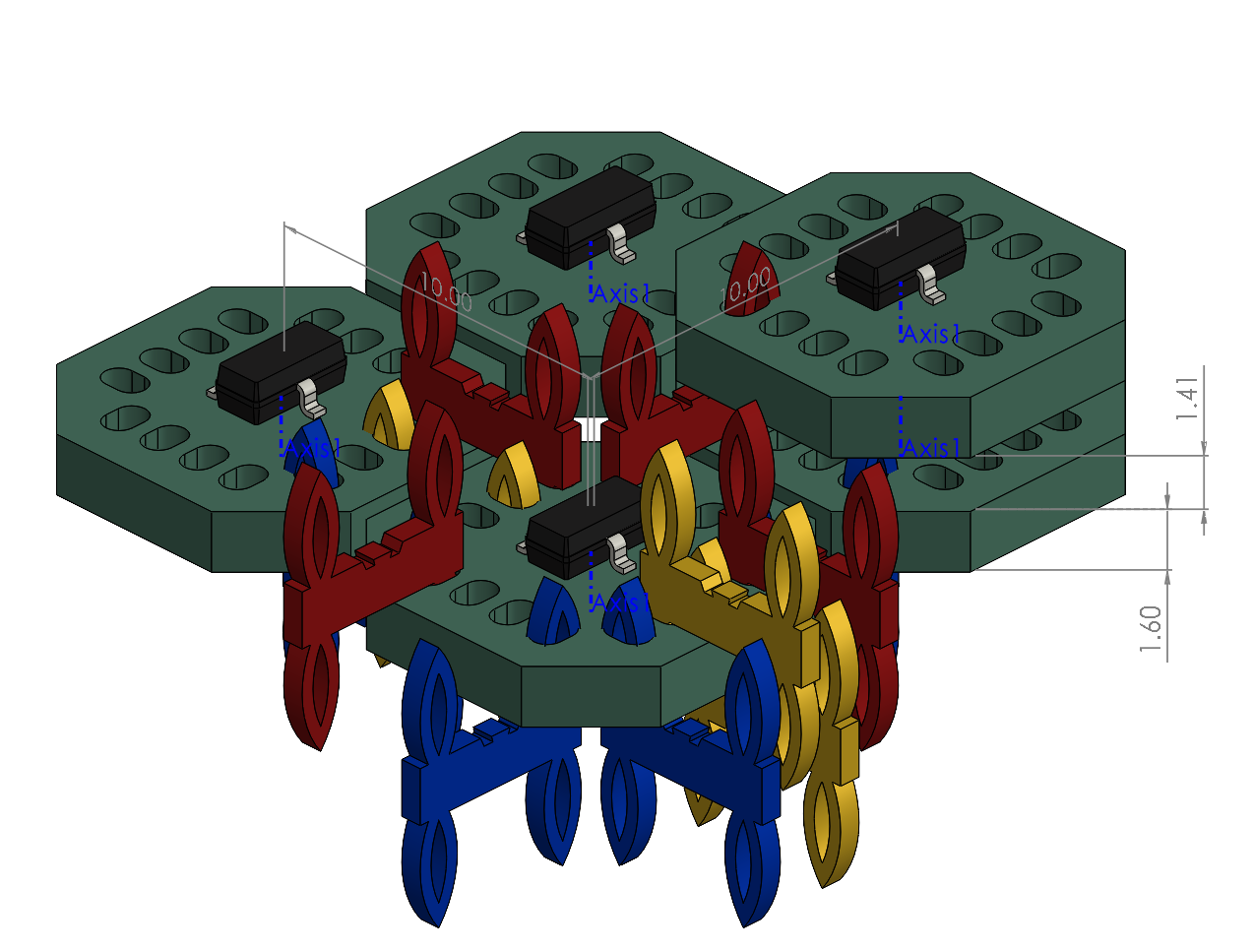
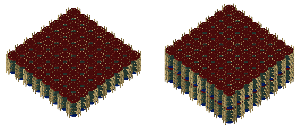
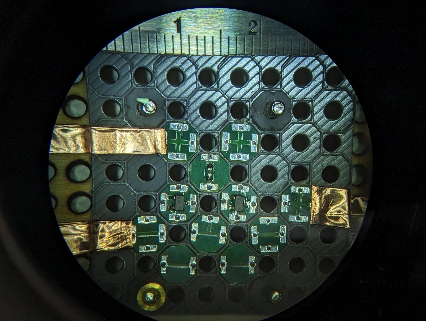
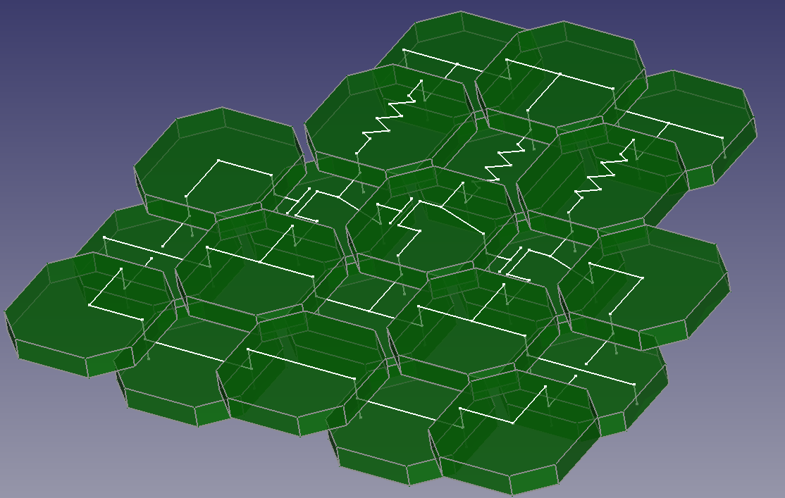
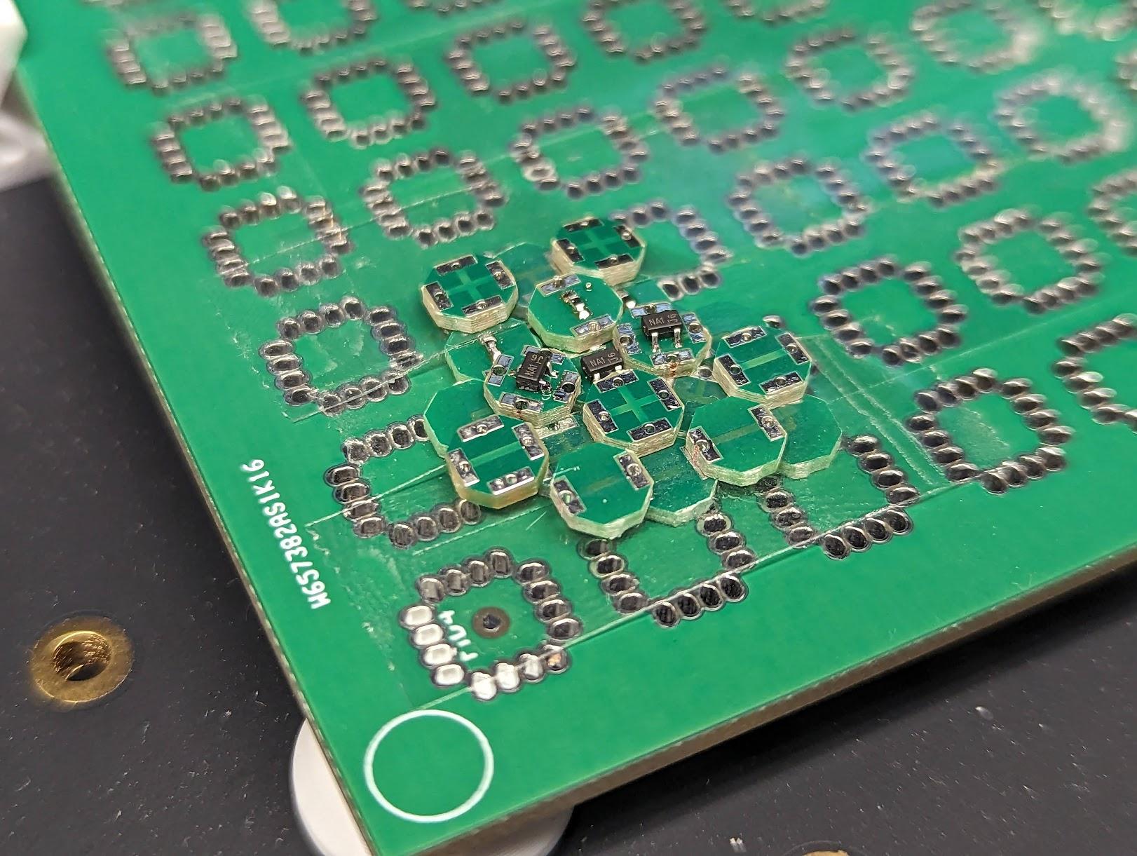
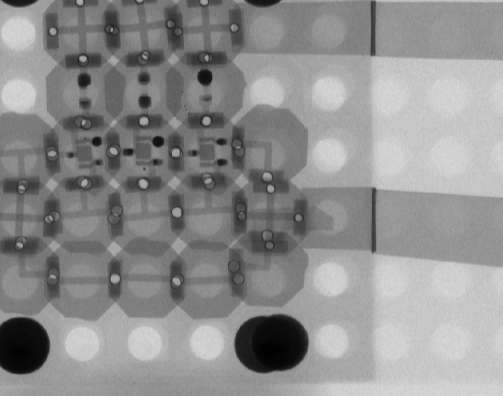
4BI represents the current active geometry in the DICE ecosystem, serving as an iteration built upon the 4B foundation, but introducing a template that works for assemblies larger than a single layer (Figure 2.13). This approach introduces significant improvements in alignment capability, though initial prototypes featured templates lacking compliant alignment features, creating a suboptimal tradeoff between pick-and-place accuracy and constraint. Subsequent iterations integrate flexures which effectively address this limitation. Compared to 4Hp, 4BI significantly improves assembly yield. Like 4B, 4BI’s alternating structure includes gaps that prevent components from interfering with neighboring tiles.
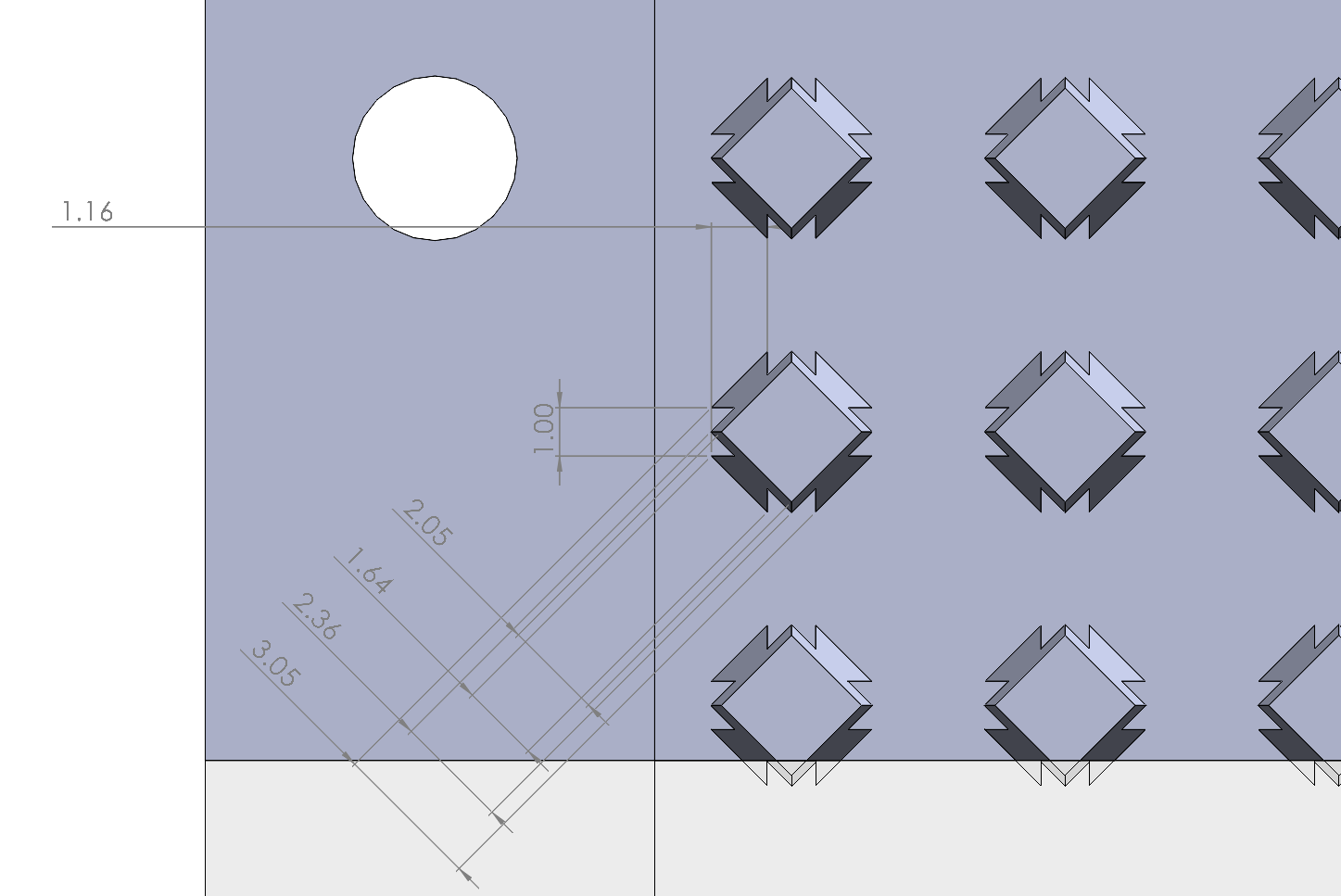
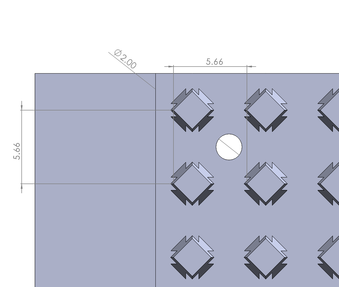
The 4BI approach (Figure 2.14) demonstrates the first version of a geometry that properly utilizes an external structure (the template and the compression cap) for mechanical constraint; this simplifies the pick-and-place process by reducing forces during component placement and relaxing tolerances, as evidenced by later versions of templates with compliant pillars.
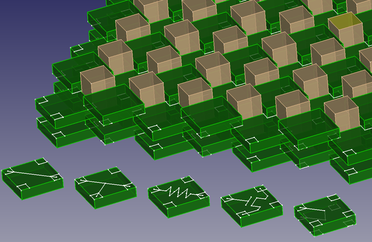
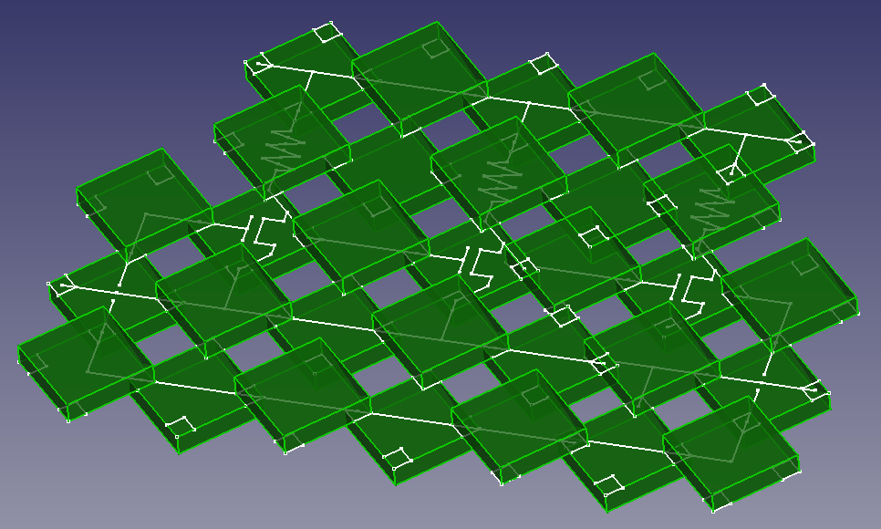
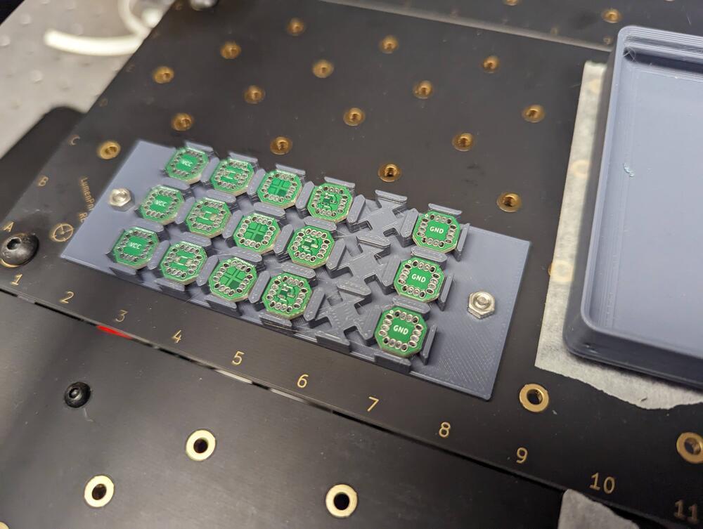
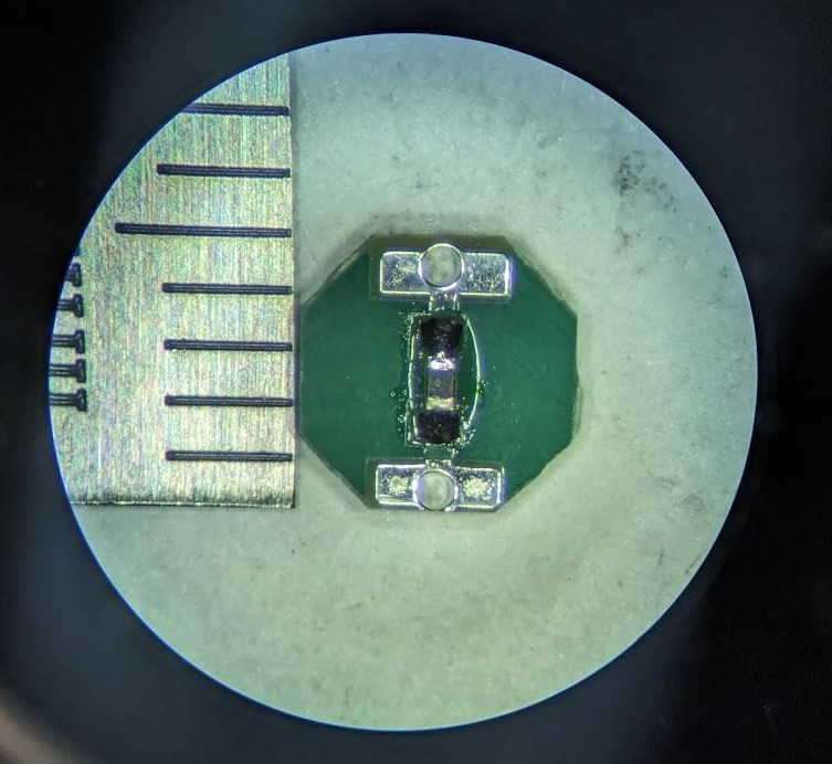
4BI tiles are all 1-layer PCBs, except for special via tiles which are 2-layer. Because dedicated power ports are no longer present in the geometry, tiles avoid the asymmetry problems present in 4Hp, however, the tradeoff is additional tiles required for power delivery within circuits. This leads to a much smaller, manageable set of tiles, which also makes scaling to larger circuit assemblies easier (Figure 2.15, Figure 2.16).
Despite these advances, 4BI introduces several notable constraints. Because the geometry introduces regular pillar features, macro-tiles have less design freedom and face fabrication challenges, since they need to accommodate holes for the pillars. Discrete joint reliability proves reliable for small circuits, but substantially worse than the 4Hp approach as circuits get larger, and the system lacks ubiquitous power distribution capabilities (for now). The 4BI approach relies heavily on global preloading to ensure reliable joints, which significantly restricts structural design freedom; this implementation strongly suggests that gaps can’t exist in the lattice structure for reliable global preload to function properly.
In a sense, 4BI is a reshuffling of forces; instead of high insertion force causing troubles during assembly, the same forces must be present post-assembly for the circuit to work.
In the following chapter, I detail the development of an automated assembly system centered around the LumenPnP capable of constructing VMD-based circuits at scale. This system represents a significant advancement beyond the manual or limited automation approaches documented in prior work. By addressing key challenges in motion control, component feeding, substrate design, and manipulation, I demonstrate how VMD elements can be assembled efficiently and reliably. The resulting system not only proves the viability of the VMD concept but establishes a pathway toward scaling to the hundreds or thousands of elements required for practical applications.
credit to Neil Gershenfeld for creating this naming scheme↩︎