4 Testing and Performance Overhead
In this chapter, we investigate joint reliability and circuit performance.
Joint reliability mostly refers to resistance of joints, as well as the Normal Force Window, which is the range of preload forces necessary for the connection to behave electrically reliably. May involve cycling tests.
Circuit performance refers to the parasitics of the assembled circuit as compared to using conventional means such as monolithic PCBs or breadboards.
Additionally, analytical performance projections are made showing smaller tiles (micrometers, nanometers) will likely lead to better performance.
4.1 Joint Reliability
4.1.1 4Hp H-eon Elements
Because 4Hp used compliant contacts in the form of the H-eon elements, it had functionally reliable contacts. During initial prototyping of H-eon elements, many parametric sweeps were made on insertion force, reusability, and insertion depth. These traits were balanced with ability to fabricate.
A key problem that led to 1-use, or sometimes simply unreliable contacts were geometries that appeared to be compliant, but instead deformed plastically after the first insertion. It was later identified that the geometry itself compromised the design; the compliant eye-of-the-needle feature was only partially formed. An iteration was created (v1.1), allowing more clearance for the feature and enabling reusability.
Unfortunately, the insertion force and connector cycles were not rigorously characterized before we switched to 4BI for its superior automatic assembly characteristics.
4.1.2 4BI Pad-to-Pad
4BI connections are formed by compressing two pads from adjacent tiles together. This is facilitated by global compression of the assembly, as described in the previous chapter. Compared to 4Hp, this approach is much easier to pick and place leading to significantly improved assembly reliability, but has been a source of intermittency for developing circuits.
4.1.3 4BI Pad Geometry
Initial experiments used rigid pillar templates, which were more tolerance sensitive, and frequently led to misalignment of neighboring pads. The geometry of the pads themselves contributed to this problem.
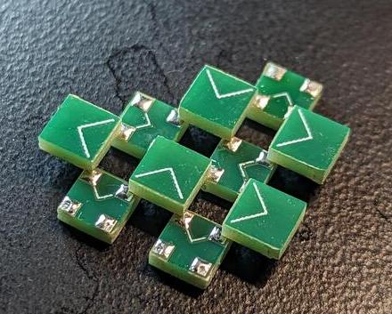
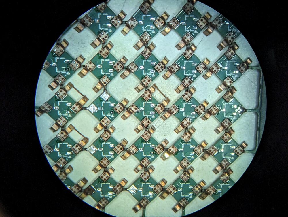
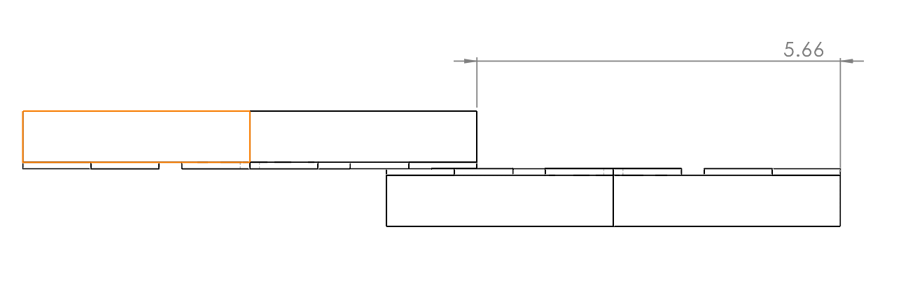
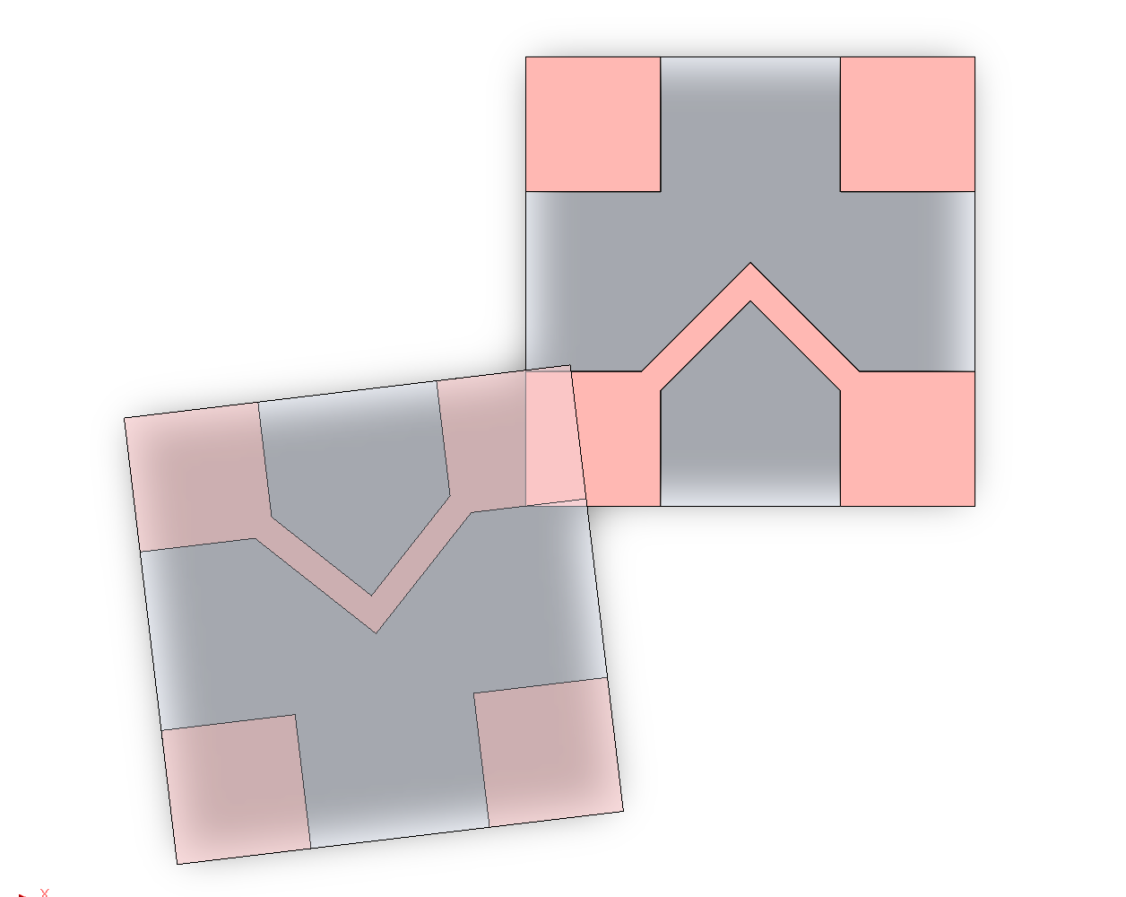
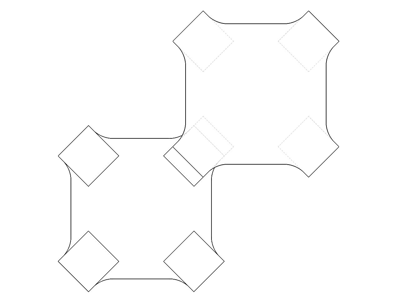
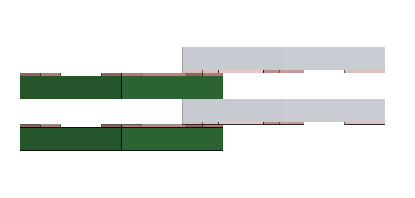
Pads were 1mm x 1mm, and increased to 1.5mm x 1.5mm for improving contact surface area (Figure 4.3), as well as enabling solder reflow tests without modifying template pitch, good for backwards compatibility with existing parts. 4BI geometry follows a 5.655mm pitch, as shown in Figure 4.2.
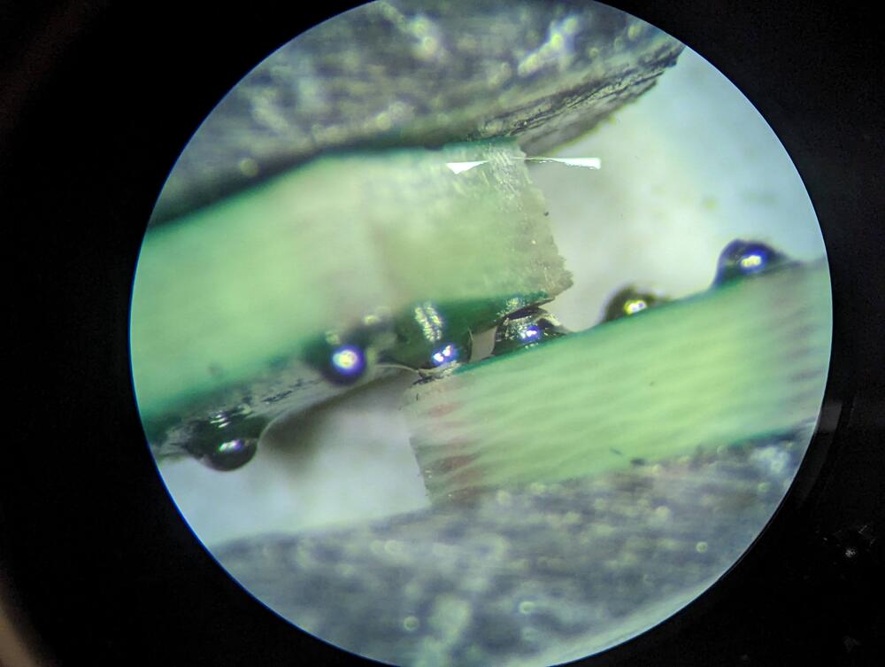
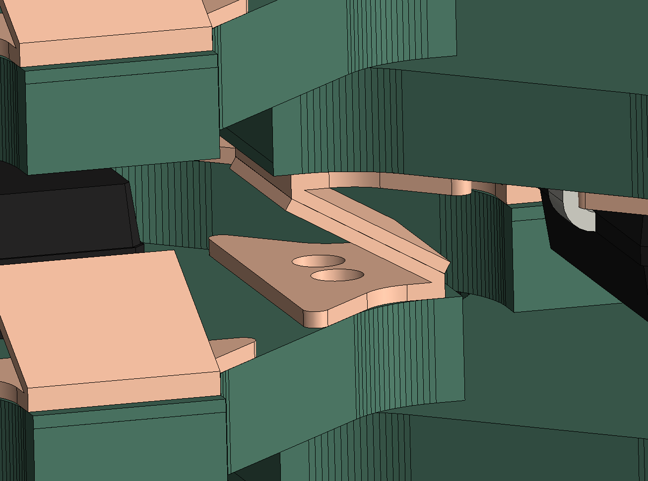
4BIc, a new variation on 4BI (the c stands for connector), was then introduced, incorporating contact geometry via leadframes. This is to reintroduce compliant contacts back into the main branch, which should be more shock and vibe tolerant than bare pads. The manner in which they interface can be seen in Figure 4.4. Unfortunately these leadframes are still experimental, and not yet complete.
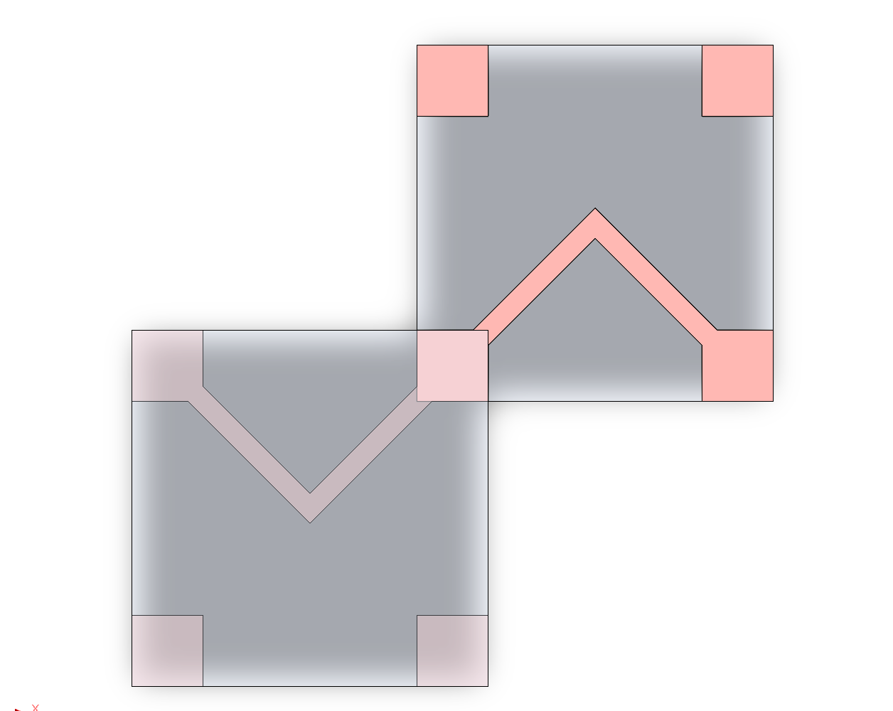
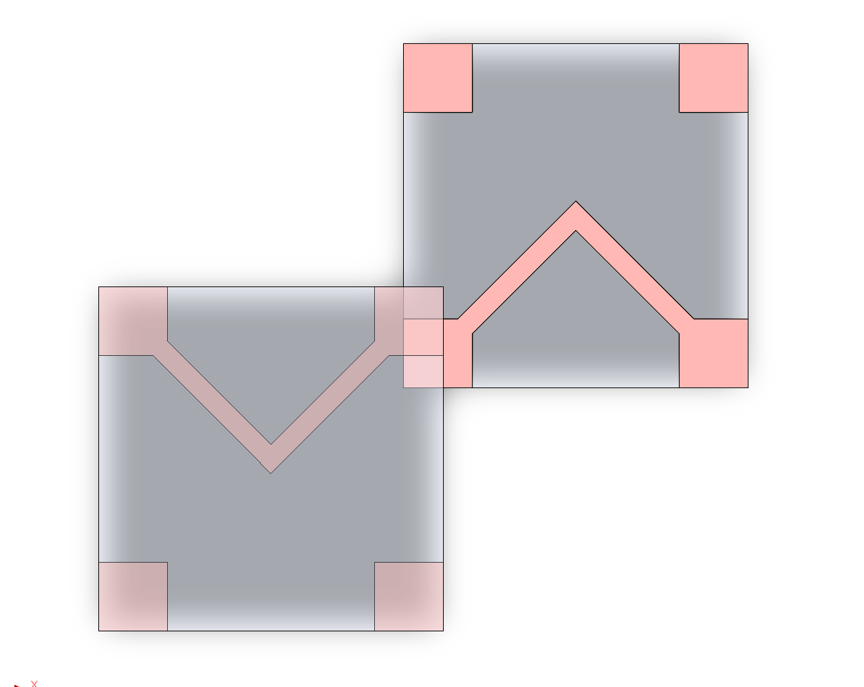
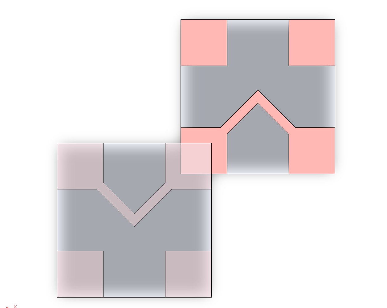
Despite lacking leadframes, the bare tiles have still been improved. Designs using the bare tiles are named 4BIc0, to indicate a variation of 4BIc without full features. To facilitate easier leadframe design, the pads were rotated such that adjacent contacts are no longer aligned by their diagonals, and instead orthogonal to each other, improving stability when neighboring tiles aren’t fully populated.
4.1.3.1 Resistance Testing
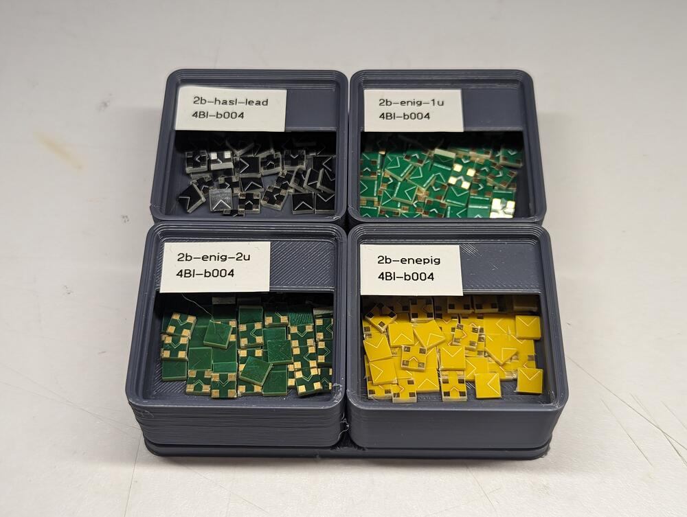
In 4BI-b004, a series of tiles were ordered with different plating finishes, which can be seen in Figure 4.1 (d). This was motivated by the idea that different material finishes with softer mechanical properties would benefit electrical performance; softer metals would deform easily and have higher contact conformity, leading to lower contact resistance. Additional connector-oriented features also influenced choice of plating finishes.
HASL is generally the go to for economic PCBs, and has been the default finish for test elements. HASL lead and unleaded perform in the same price range and performance domain, so only HASL lead was used. ENIG and ENEPIG were selected for their electrical properties, resilience to oxidation, and wear characteristics. Copper was quickly excluded due to quick oxidation. Phosphor Bronze (C510) is a copper alloy typically used for connector contacts requiring spring properties, great for compliant contact designs. It isn’t readily available as a plating finish from PCB houses like PCBWAY, but easily available as sheet stock from vendors such as McMaster-Carr.
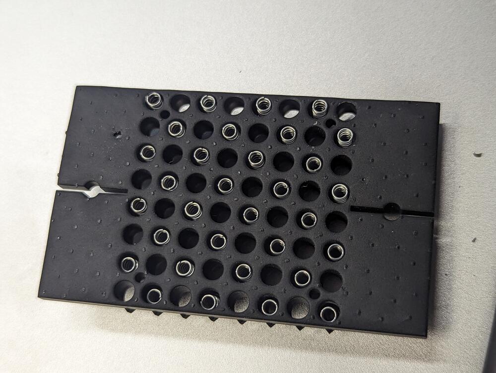
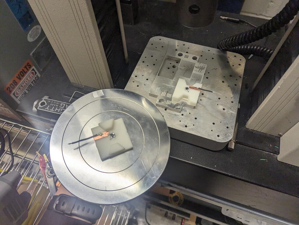
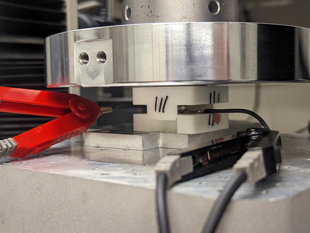
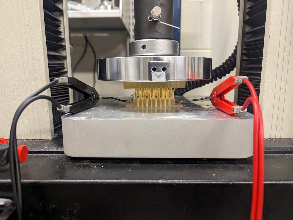
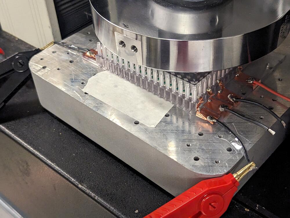
A test setup was then devised to test individual tile pad-on-pad performance. A 3d printed jig (Form 4 Rigid 4k) was used to hold a tile each, and wired to a 4-wire resistance testing setup. This design under test (DUT) would then be subject to an instron, used to compress two adjacent pads from each tile together. Because the instron uses an offline computer, system clocks were used to synchronize resistance and load measurements, accurate to a second.
Each jig holding the tile is loosely constrained in x and y using alignment features, also commonly used for mold making and other tooling registration steps, such as the ones used to fabricate 4BIc. This was designed this way to avoid potential binding or other overconstraint conditions that would compromise the experiment, ensuring only normal forces between the two pads are measured.
Pyralux copper tape was used to add well-constrained, solderable conductive paths to break out the tile connections to decouple cable strain from the tile, which was fixed in place using UV glue. The test jigs can be seen in Figure 4.5.
To install the jigs into the instron, double-sided nitto tape was used to affix the bottom and top halves of the jig to the base and loadcell. It was necessary to affix the bottom to a piece of flat mic6 stock, since the wire strain from the kelvin probes would tilt the setup, oriented the wrong way. The mic6 stock was left loose, to underconstrain the system so the registration features can be aligned. This can be seen in Figure 4.6.
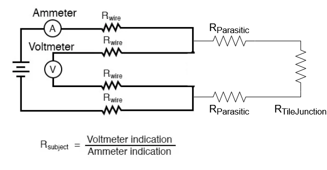
The breakout assembly (kelvin probe -> wire -> solder -> copper tape -> solder -> tile -> tile on-board resistance) series resistance was measured using a 4-wire setup prior to the experiments, such that parasitic resistances are accounted for while measuring resistance of the pad-to-pad joint itself. This parasitic can be seen in the test setup schematic, shown in Figure 4.7. This parastic resistance measurement was conducted on each of the two halves of the jig (top, bottom), and there were 4, for a total of 8 separate measurements.
| Sample | Parasitic Resistance Sum (Ω) | Parasitic Resistance Sum (mΩ) |
|---|---|---|
| 1 | 0.01898 Ω | ~18.98 mΩ |
| 2 | 0.02345 Ω | ~23.45 mΩ |
| 3 | 0.03004 Ω | ~30.04 mΩ |
| 4 | 0.02669 Ω | ~26.69 mΩ |
Then, each sample was subject to testing, which displaced at a rate of 2mm/min to the end condition of 100N compressive force. Data can be seen in Figure 4.8.
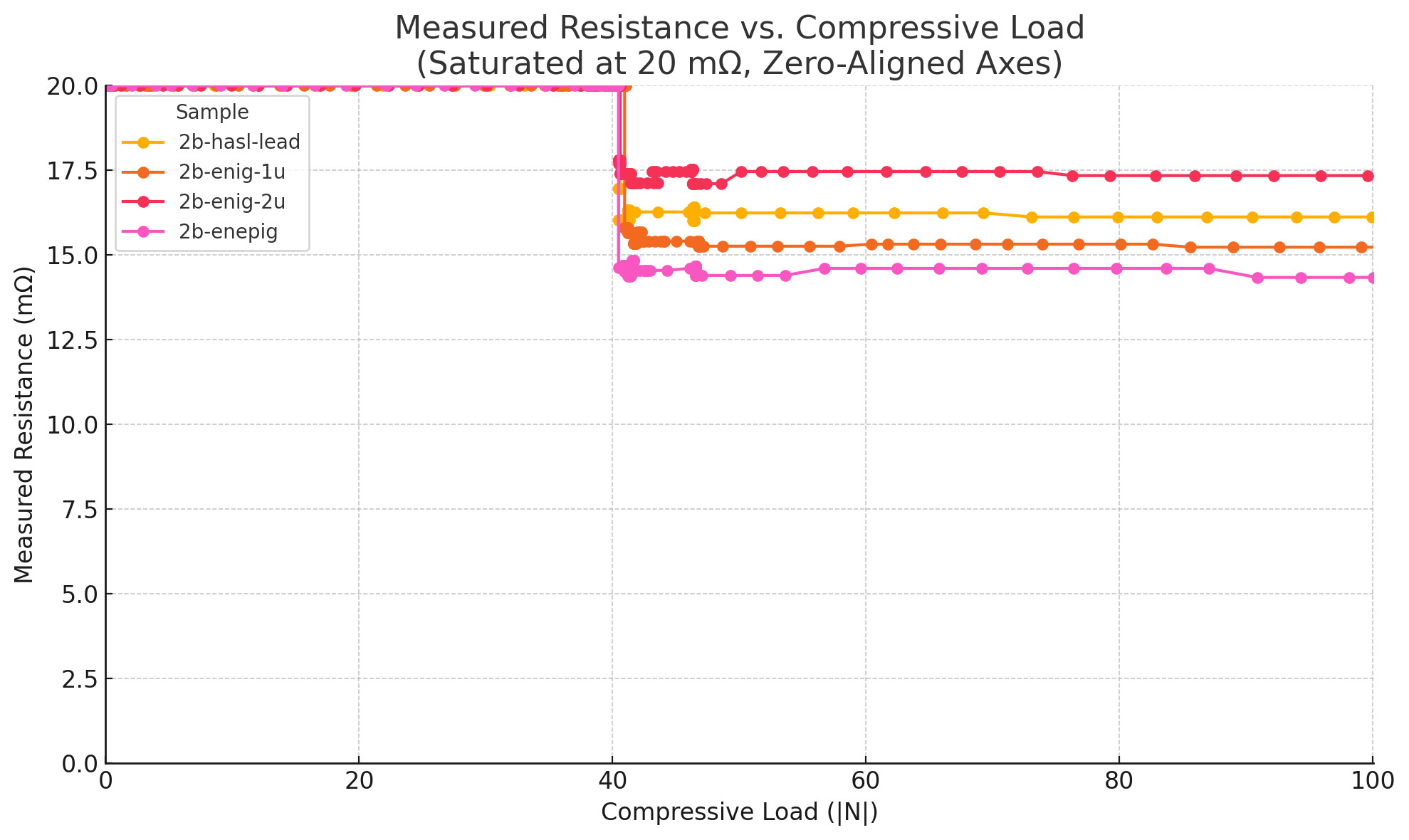
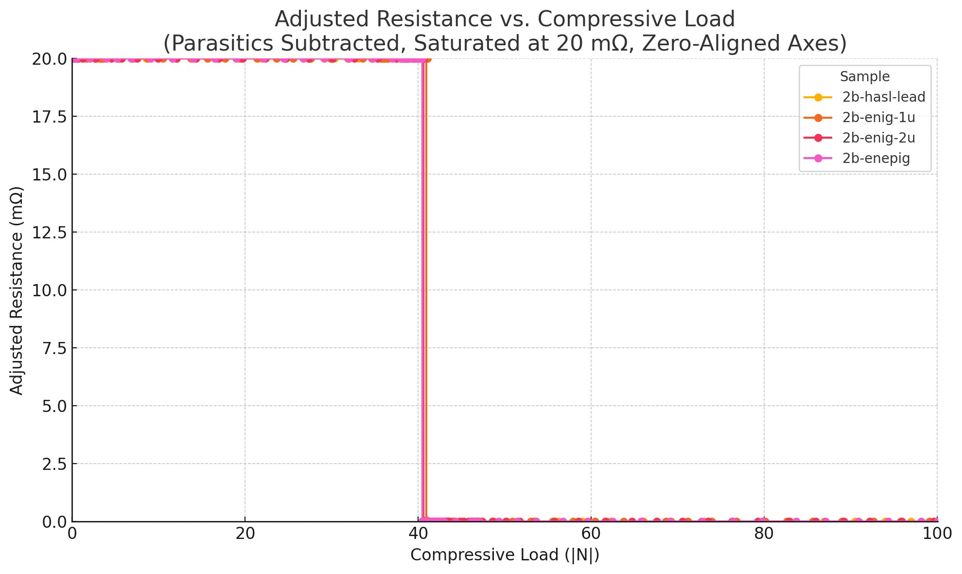
Subtracting the parasitics netted negative values, suggesting that the resistances in the system for individual joints are below the noise floor of my measuring equipment. This makes comparing finishes purely on resistance impossible, except that all of the finishes appear to perform adequately. However, the data does provide insight into activation forces. The Normal Force Window of all 4 samples was >50N, with an intermittent but still acceptable period from 40-48N. This can be seen in Table 4.1.
| Sample | Min Resistance (mΩ) | Stable Force Range ( |
|---|---|---|
| 2b-hasl-lead | 16.01 | 50.15 N → 101.50 N |
| 2b-enig-1u | 15.23 | 48.72 N → 100.55 N |
| 2b-enig-2u | 17.11 | 48.60 N → 101.03 N |
| 2b-enepig | 14.34 | 49.32 N → 100.07 N |
4.1.3.2 Cycling
For testing reusability, a cycling test is necessary to see how many cycles a connector contact can undergo before behaving differently.
A preliminary cycling test on the HASL-lead sample was conducted to evaluate joint reusability. However, the test inadvertently operated under a strain-controlled mode rather than force- or displacement-controlled cycling, resulting in peak compressive loads exceeding 400 N and triggering the 500 N cutoff condition, which caused the sample to fail after four cycles. While this result highlights the sensitivity of the joint to over-compression and underscores the need for controlled force cycling in future tests, it does not reflect performance under nominal operating conditions. Future work will focus on properly constrained tests required to determine realistic reuse lifetimes.
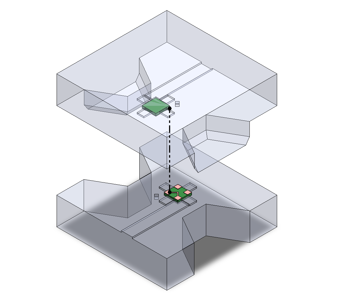
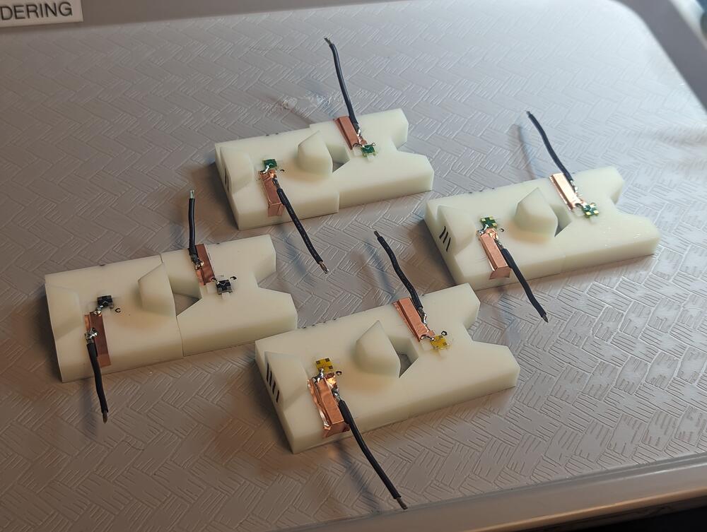
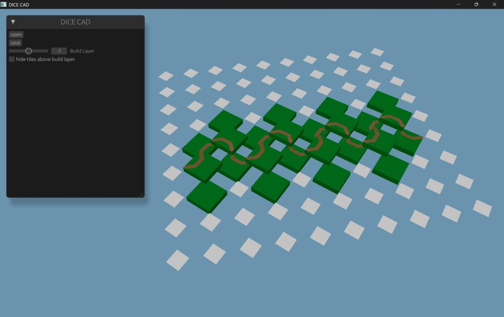
For a more realistic scenario, a continuity test was implemented using 4BI-b004-2b tiles, to create a “snaking” trace across one of the 8x8 templates, as seen in Figure 4.9. In total, 14 joints were used in the continuity test. Due to time, this test was not conducted and will also be left for future work.
4.2 Circuit Performance
Multiple circuits were built over the course of development. These spanned from basic benchmarking tests, such as continuity tests, then simple operational circuits such as ring oscillators, and finally logical circuits like nand gates and adders, with the intent to eventually build an entire RISC-V CPU.
4.2.1 Ring Oscillators
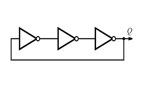
The ring oscillator has almost been the functional hello-world of each geometry. It demonstrates basic conductivity, some functional components, and a quick way to benchmark relative parasitics through the resonant frequency of the circuit. It is a circuit made of an odd number of inverters connected in a loop, where the signal continuously toggles due to propagation delays, producing a periodic square wave.
A 4Hp implementation can be seen in Figure 4.10. An equivalent ring oscillator design has been made for 4BIc0 (Figure 4.10 (d)), but it has yet to be tested.
4.2.2 Logic Gates
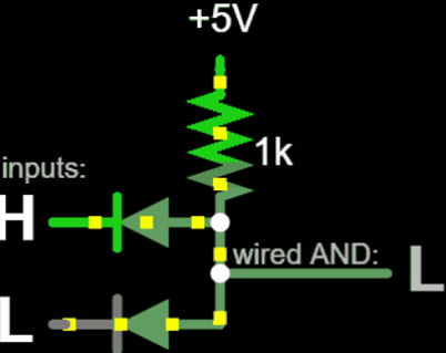
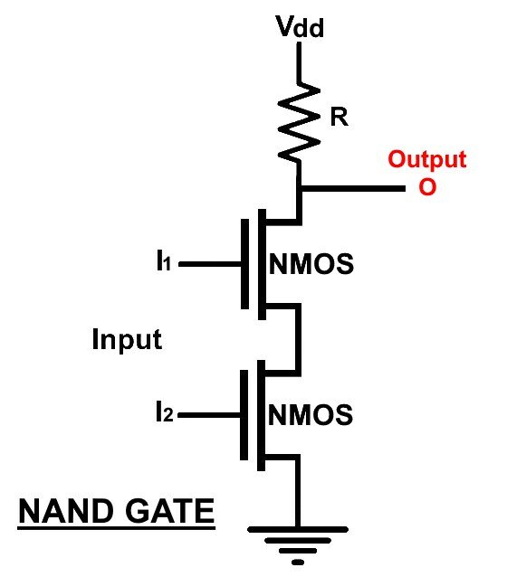
Basic logic gates, as shown in Figure 4.11, can be put together to build many other complex functional blocks, such as half-adders and full-adders, to an ALU, and ultimately culminating in a computer. NANDs (or ANDs in diode logic) are a very commonly used logic gate. We use NANDs and NORs in our more complex circuits.
4.2.3 Full Adders
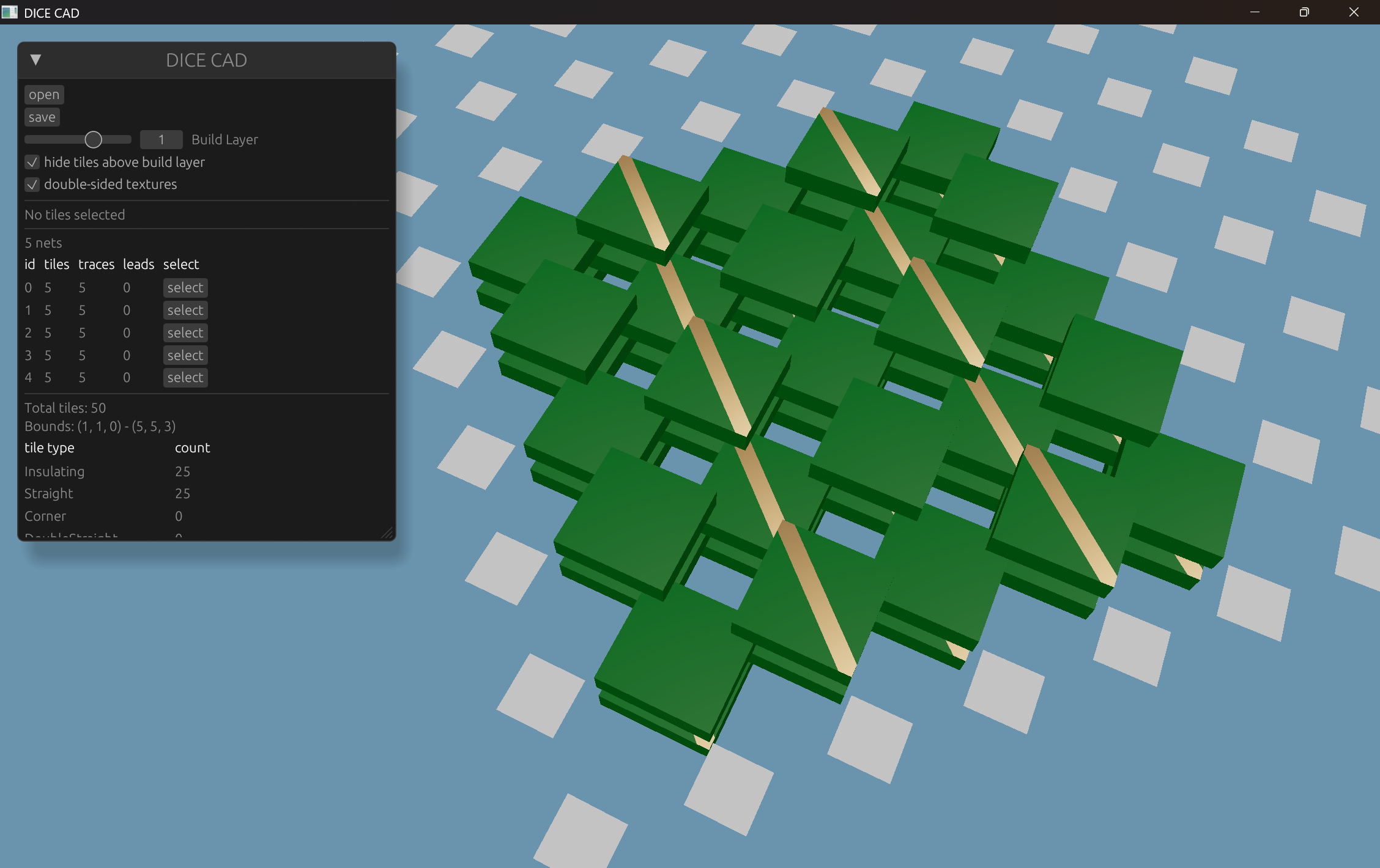
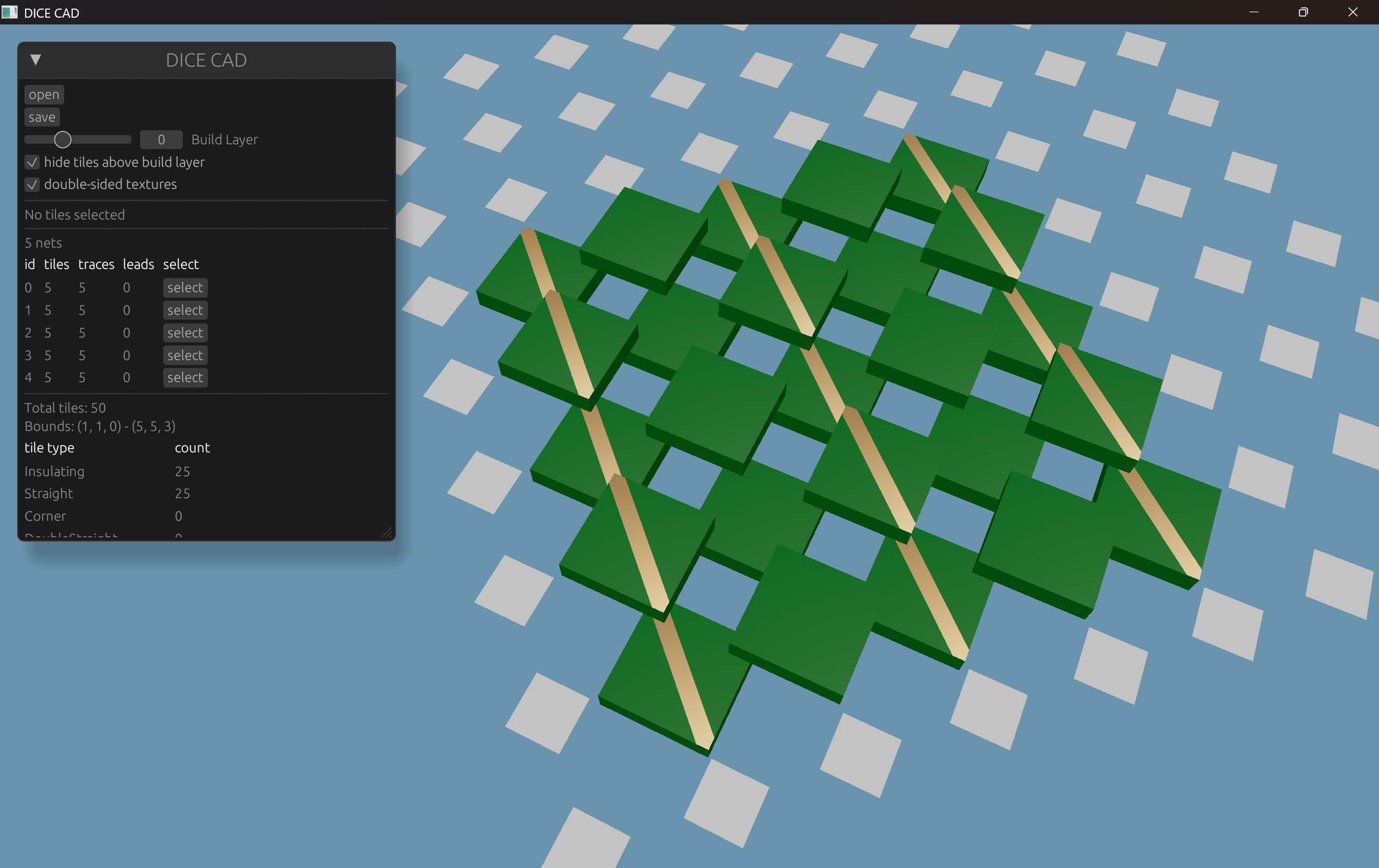
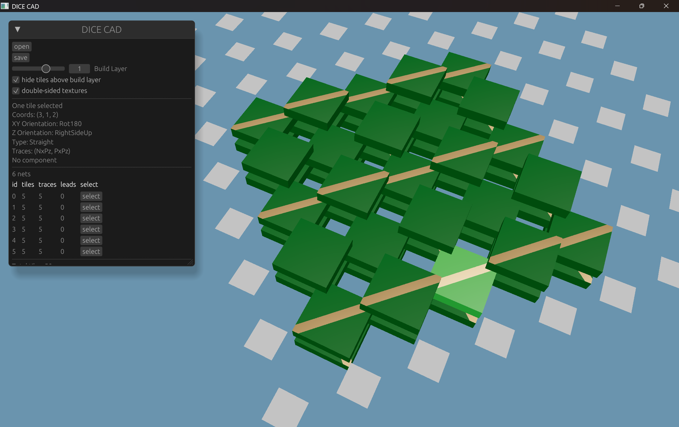
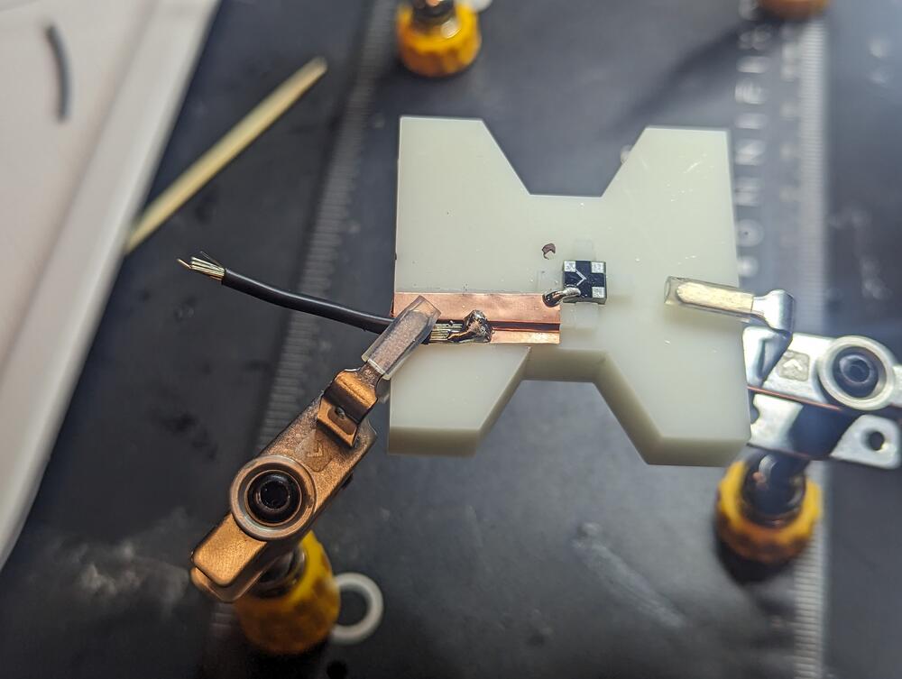
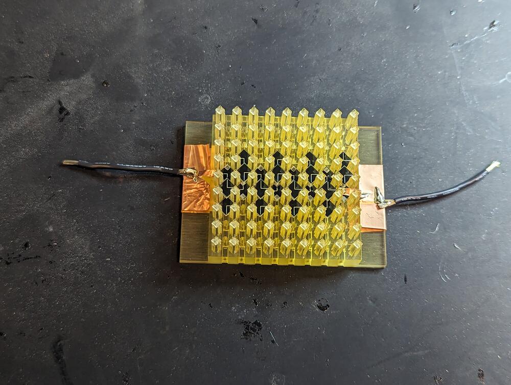
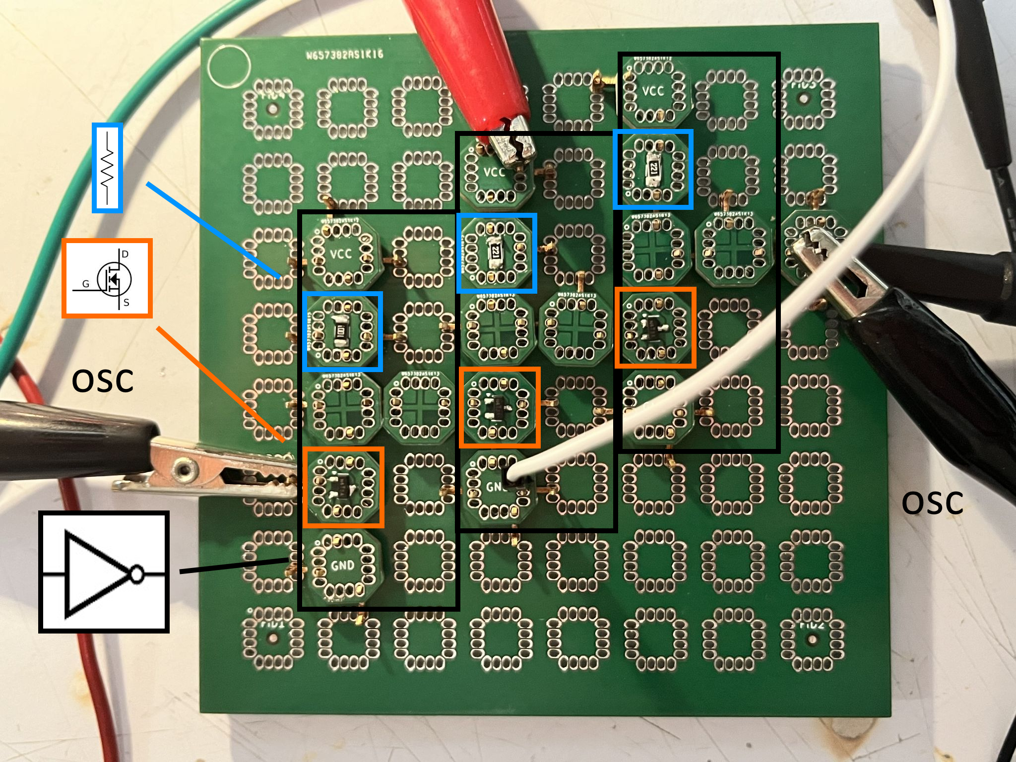
A 4Hp full-adder circuit (Figure 4.13 (a), Figure 4.13 (b)) was manually constructed by Shravika Pendyala, which itself is composed of two half-adders assembled on 8x8 macro tiles. This represents a more complex logic application circuit.
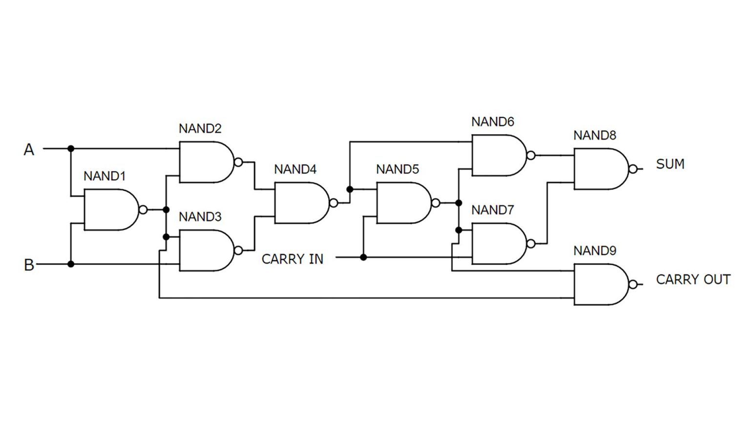
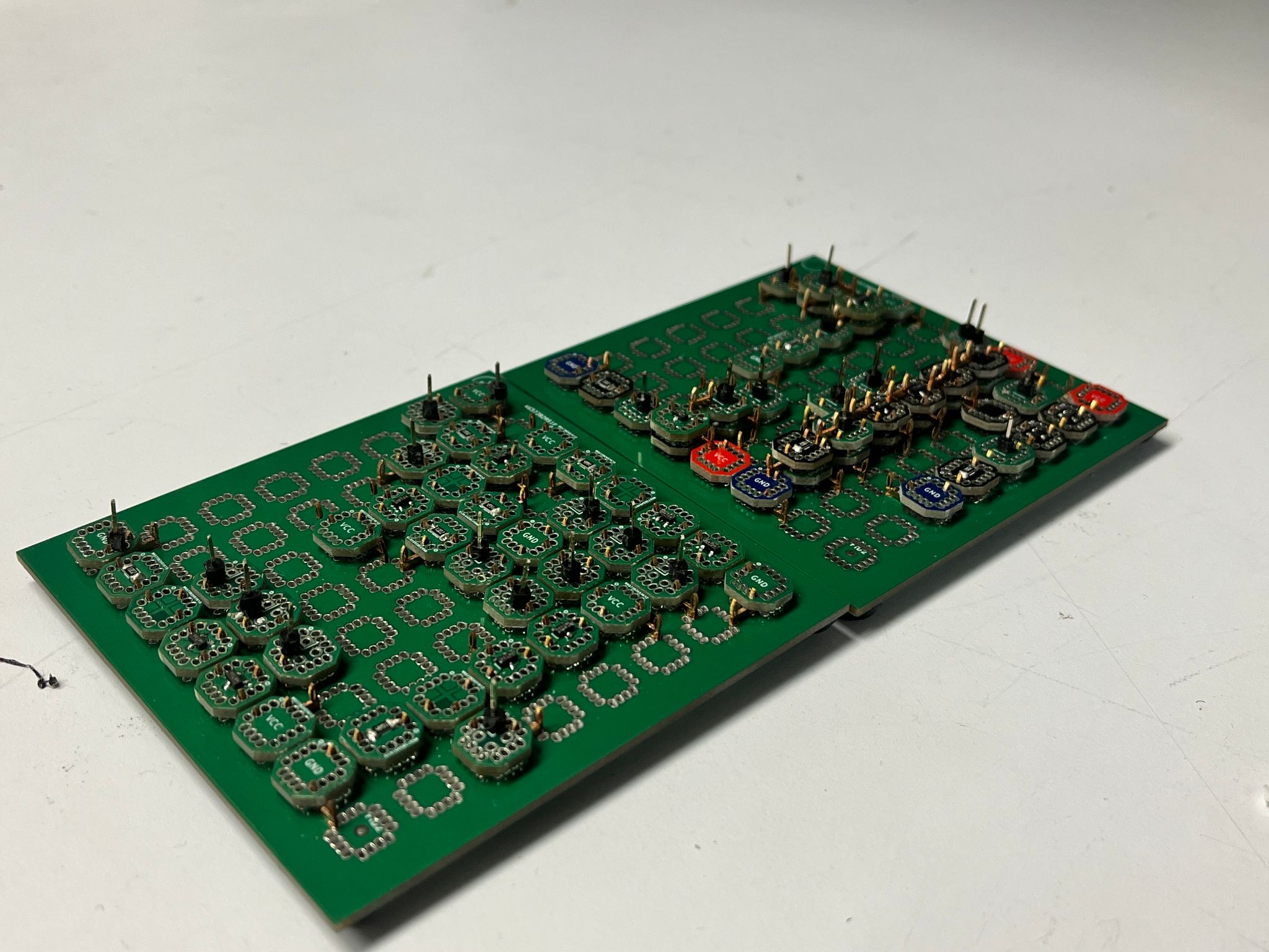
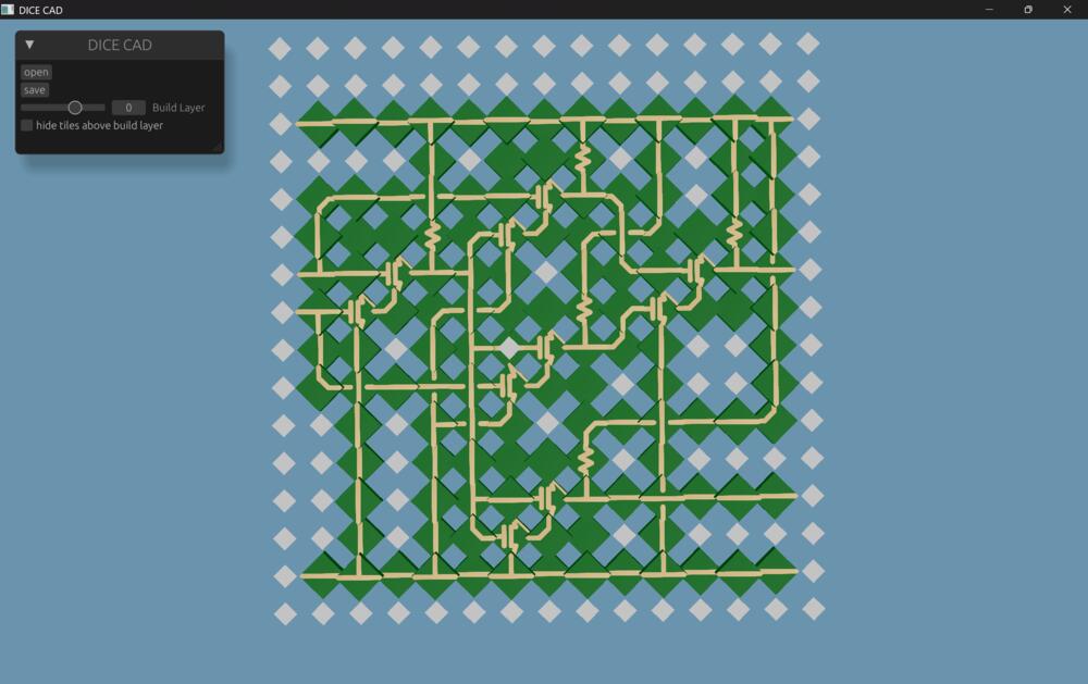
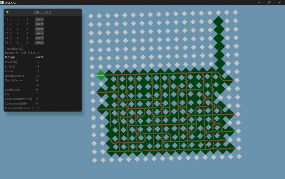
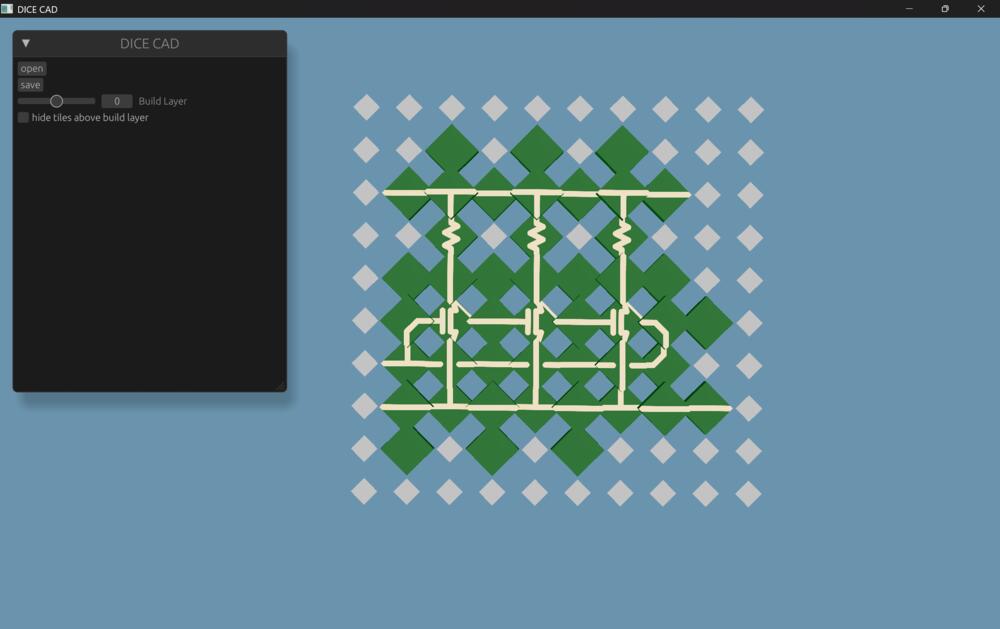
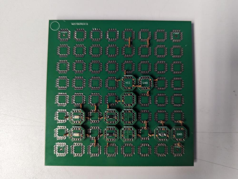
In 4BIc0, I designed a half adder in dice-cad (Figure 4.13 (c)). However, given the comparable tile counts, Erik and I opted to carry out implementation of a full adder instead (Figure 4.13 (d)). A stackable full adder (Figure 4.13) was designed by Erik Strand using dice-cad, which I then modified by breaking out connections and fitting it to the 16x16 template. Additional filler tiles were added to improve mechanical stability. Setup was done to make the pattern pick and placeable, but due to time, I manually assembled the circuit shown here. This took about ~55 minutes, and was done using a straight tweezer.
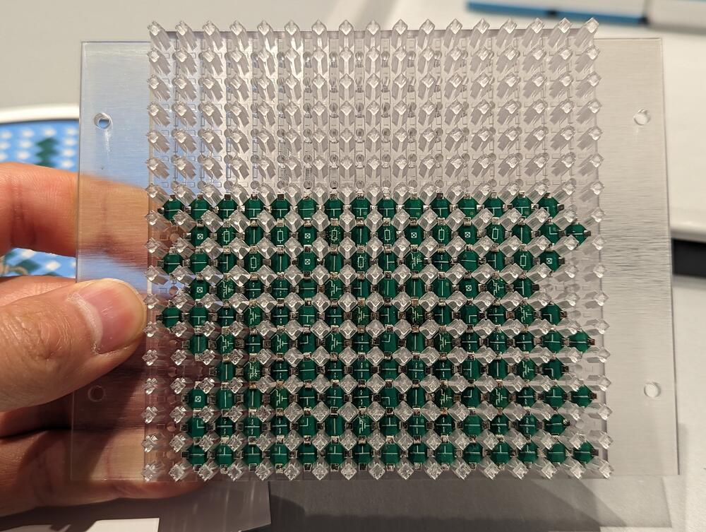
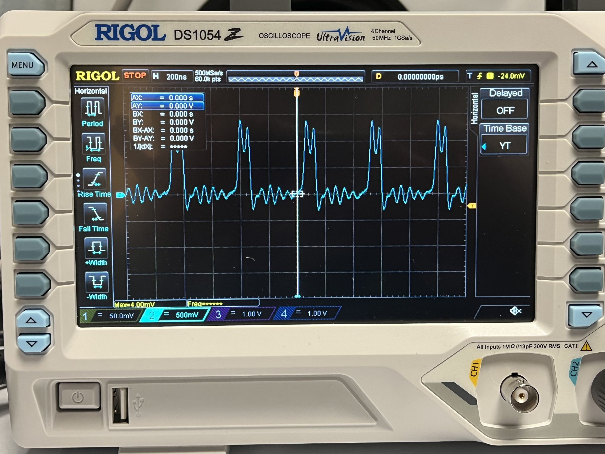
For preliminary tests, the power and ground nets were measured for continuity and resistance; the Normal Force Window required for activation was >100N. The ground and power net measured ~0.1mOhms. Unfortunately, the center circuitry appears to be intermittent, and requires further work to diagnose. There are multiple potential issues preventing the circuitry from working reliably, one possibility is difficulty guaranteeing even force distribution due to warping of the resin template and cap, or non-planarity from the tiles and their stackup, or both.
Discretizing the cap itself and redesigning it for additional compliance (or adding a compressible layer) are potential solutions to the above problems, but the lack of compliance from the tiles themselves may make required forces difficult. Even after applying some of these solutions and increasing to 300N didn’t show improvement.
This is likely where 4BIc could help the most; compliant leaf-spring contacts on each joint interface may help evenly distribute forces while forcing contact at forces well below bare 4BI contact pads, further investigation and process development here is required to scale functional circuits. In the next chapter, I will talk about the manufacturing process for 4BIc, which further builds upon 4BI’s ease of assembly with ease of conductivity.
4.3 Scaling Performance Projections
As our geometry shrinks from the millimeter to the micrometer regime, we assume that the switching speed in our architecture is limited primarily by the LC time constant instead of the RC time constant, due to \(R\) decreasing as tile size and trace length shrinks:
\[ t_{\text{rise}} \sim \sqrt{LC} \quad \text{rather than} \quad t_{\text{rise}} \sim RC \]
To estimate performance of tile-scale interconnects under geometric scaling, we approximate the key electrical parameters using simplified analytical models. These derivations assume uniform tile side length \(s\), a coverage factor \(\alpha\) representing the fraction of surface area occupied by traces or pads, and a gap \(d\) between tiles.
4.3.1 Capacitance
We approximate the parasitic capacitance between two vertically adjacent tiles (also known as broadside-coupling [1]) using the parallel plate capacitor model, modified by a coverage factor:
\[ C = \frac{\varepsilon_0 \varepsilon_r A}{d} \qquad \text{with} \qquad A = \alpha^2 s^2 \] \[ \boxed{C = \frac{\varepsilon_0 \varepsilon_r \alpha^2 s^2}{d}} \]
where:
- \(C\): Capacitance between tiles [F]
- \(s\): Tile side length [m]
- \(\alpha\): Surface coverage factor (fraction of tile face covered by conductive traces or pads)
- \(d\): Gap between adjacent tiles [m]
- \(A\): Effective overlapping conductive area between tiles, \(A = \alpha^2 s^2\) [m\(^2\)]
- \(\varepsilon_0\): Vacuum permittivity (\(\approx 8.85 \times 10^{-12}\) F/m)
- \(\varepsilon_r\): Relative permittivity of dielectric between tiles (dimensionless)
The surface coverage factor \(\alpha\) represents the fraction of each tile face covered by conductive material, including traces and pads. \(\alpha^2\) is used in the capacitance calculation to include the statistical expectation of overlap between two independent conductive patterns on vertically neighboring tile surfaces.
If each surface has \(\alpha s^2\) of metallized area, then the expected overlapping area between two randomly oriented or anisotropically routed layers (e.g. orthogonal traces) is:
\[ A_{\text{overlap}} = \alpha^2 s^2 \]
This arises from the probability that a point on one surface is metallized \((\alpha)\) and that the corresponding point on the opposing surface is also metallized \((\alpha)\), resulting in \(\alpha \cdot \alpha = \alpha^2\) of the total area.
In contrast, if the routing patterns are perfectly aligned (e.g. solid pads on both sides or repeated structures), a single factor \(\alpha\) may suffice:
\[ A_{\text{overlap}} = \alpha s^2 \]
However, realistic 4BI designs may see a variety of routing tiles being used; the uncorrelated or orthogonal layout assumption is more accurate. Thus, the model adopts:
\[ \boxed{C = \frac{\varepsilon_0 \varepsilon_r \alpha^2 s^2}{d}} \]
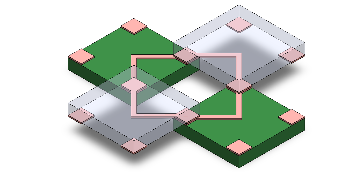
An additional modifier to the original parallel plates capacitance equation requires looking closer at the tile stackup. To realistically map this model to 4BI, the dielectric stackup between plates becomes more complex. As shown in Figure 4.14, the closest valid geometric arrangement features an air gap and solid substrate (typically FR4 or silicon) between the plates, properly isolating the nets. This arrangement can be modeled as a pair of capacitors in series:
\[ \frac{1}{C_{\text{total}}} = \frac{1}{C_1} + \frac{1}{C_2} = \frac{d_1}{\varepsilon_0 \varepsilon_{r1} A} + \frac{d_2}{\varepsilon_0 \varepsilon_{r2} A} \]
where:
- \(d_1\), \(\varepsilon_{r1}\): thickness and relative permittivity of the first dielectric (e.g. air)
- \(d_2\), \(\varepsilon_{r2}\): thickness and relative permittivity of the second dielectric (e.g. substrate)
- \(A = \alpha^2 s^2\): effective overlapping area
This leads to the compact form:
\[ \boxed{ C = \frac{\varepsilon_0 \alpha^2 s^2}{\frac{d_1}{\varepsilon_{r1}} + \frac{d_2}{\varepsilon_{r2}}} } \]
Practically, this model has implications on channel routing especially when layers start to stack. For example, avoiding overlap by staggering parallel traces on adjacent layers, or minimizing overlap by running traces orthogonal to each other. Additionally, adding shielding through ground pours between layers can help confine capacitive coupling.
4.3.2 Inductance
For inductance, we model the loop formed by a signal trace and its return path (via neighboring tiles or vias) as a square current loop of side length \(s\):
\[ L \approx \mu_0 \cdot s \cdot \left[ \ln\left( \frac{2s}{r} \right) - 0.774 \right] \quad \Rightarrow \quad \boxed{L \sim \mu_0 \cdot s} \]
where:
- \(L\): Inductance of signal-return loop [H]
- \(\mu_0\): Vacuum permeability (\(= 4\pi \times 10^{-7}\) H/m)
- \(s\): Tile side length (loop length) [m]
- \(r\): Effective trace width or conductor radius [m]
4.3.3 Resonance Frequency
The natural resonance frequency of the LC circuit formed by the parasitic elements is:
\[ f_0 = \frac{1}{2\pi\sqrt{LC}} \sim \frac{1}{2\pi} \cdot \sqrt{ \frac{d}{\mu_0 \varepsilon_0 \varepsilon_r \alpha^2 s^3} } \quad \Rightarrow \quad \boxed{f_0 \propto \frac{1}{s^{3/2}}} \]
where:
- \(f_0\): Resonance frequency of LC circuit [Hz]
- \(L\): Inductance of signal-return loop [H]
- \(C\): Capacitance between tiles [F]
4.3.4 Capacitive Switching Energy
Assuming a voltage swing \(V\) per logic transition, the energy dissipated in charging the capacitance is:
\[ \boxed{E_{\text{cap}} = \frac{1}{2} C V^2 = \frac{1}{2} \cdot \frac{\varepsilon_0 \varepsilon_r \alpha^2 s^2}{d} \cdot V^2} \]
where:
- \(E_{\text{cap}}\): Capacitive energy dissipated per logic transition [J]
- \(C\): Capacitance between tiles [F]
- \(V\): Voltage swing per logic transition [V]
4.3.5 Projections from 10mm down to 10nm
Using the following constants:
- \(\varepsilon_0 = 8.85 \times 10^{-12} \ \mathrm{F/m}\) — Vacuum permittivity
- \(\mu_0 = 4\pi \times 10^{-7} \ \mathrm{H/m}\) — Vacuum permeability
- \(\varepsilon_{r1} = 1.0\) — Relative permittivity of air
- \(\varepsilon_{r2} = 3.0\) — Relative permittivity of substrate (e.g. FR4)
- \(\alpha = 0.5\) — Surface coverage factor
- \(V = 1.0 \ \mathrm{V}\) — Voltage swing
And sweeping these equations from s = 10mm to 10nm, we see the following:
For keeping tile dimensions proportional and shrinking tiles:
Capacitance (\(C\)) scales linearly with \(s\): \[ C \propto \frac{s^2}{d} \propto \frac{s^2}{s} = s \] Shrinking tiles reduces capacitance proportionally.
Inductance (\(L\)) also scales linearly with tile size: \[ L \propto s \] This follows from loop inductance scaling with geometric size.
LC Product (\(LC\)) scales quadratically: \[ LC \propto s \cdot s = s^2 \quad \Rightarrow \quad f_0 \propto \frac{1}{\sqrt{LC}} \propto \frac{1}{s} \] Resonance frequency increases linearly with decreasing tile size.
Capacitive Switching Energy (\(E\)) scales linearly: \[ E = \frac{1}{2} C V^2 \propto s \] Resulting in reduced energy per switch at smaller tile sizes.
These trends support the conclusion that miniaturization improves signal bandwidth and reduces energy dissipation, with no parasitic term that worsens under scale in this model. The dielectric model reflects realistic fabrication constraints and validates the use of LC-dominated timing models for high-speed, small-scale tile architectures.
If we vary surface coverage by sweeping \(\alpha\) from 0.1 to 0.9:
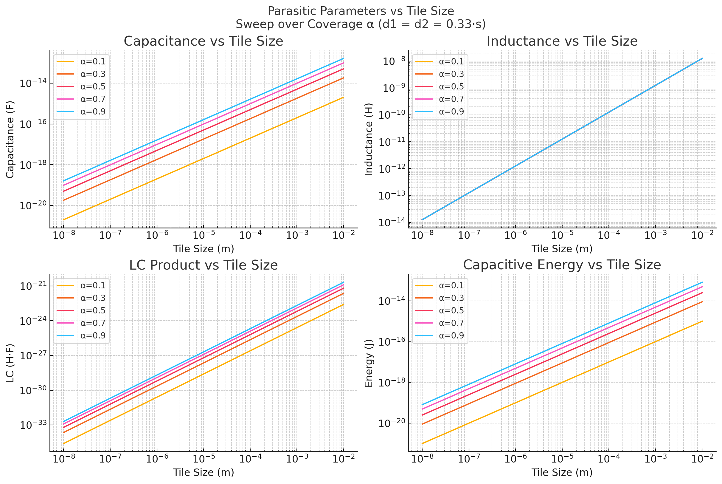
We see the following:
Capacitance (\(C\)) increases quadratically with coverage: \[C \propto \alpha^2\] This reflects the statistical overlap area between partially metallized tiles. Increasing trace or pad area significantly raises parasitic capacitance.
Inductance (\(L\)) is independent of \(\alpha\): \[L \propto s\] Because loop inductance is set by geometric scale and return path, not coverage.
LC Product (\(LC\)) increases with \(\alpha^2\): \[LC \propto \alpha^2 s^2 \quad \Rightarrow \quad f_0 \propto \frac{1}{\alpha s}\] As coverage increases, resonance frequency decreases, setting a tradeoff between signal density and bandwidth.
Capacitive Switching Energy (\(E\)) also increases with \(\alpha^2\): \[E = \frac{1}{2} C V^2 \propto \alpha^2\] Denser routing incurs a power cost, suggesting a need to balance coverage with energy efficiency.
These results demonstrate that although higher \(\alpha\) improves connectivity and potentially robustness, it comes at the cost of slower transitions and greater energy consumption. Optimal tile designs must consider \(\alpha\) as a critical tuning parameter for performance and power tradeoffs, for example through Joule heating.
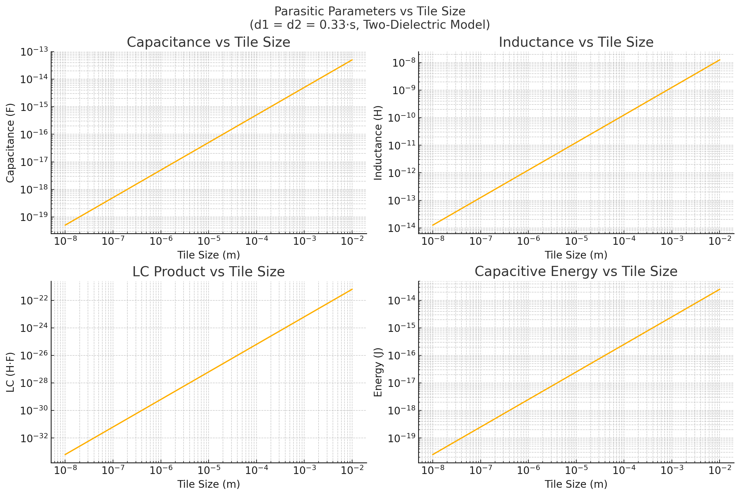
Finally, we sweep dielectric layer thickness \(d_1 = d_2 = k \cdot s\) from \(k = 0.1\) to \(k = 0.33\):
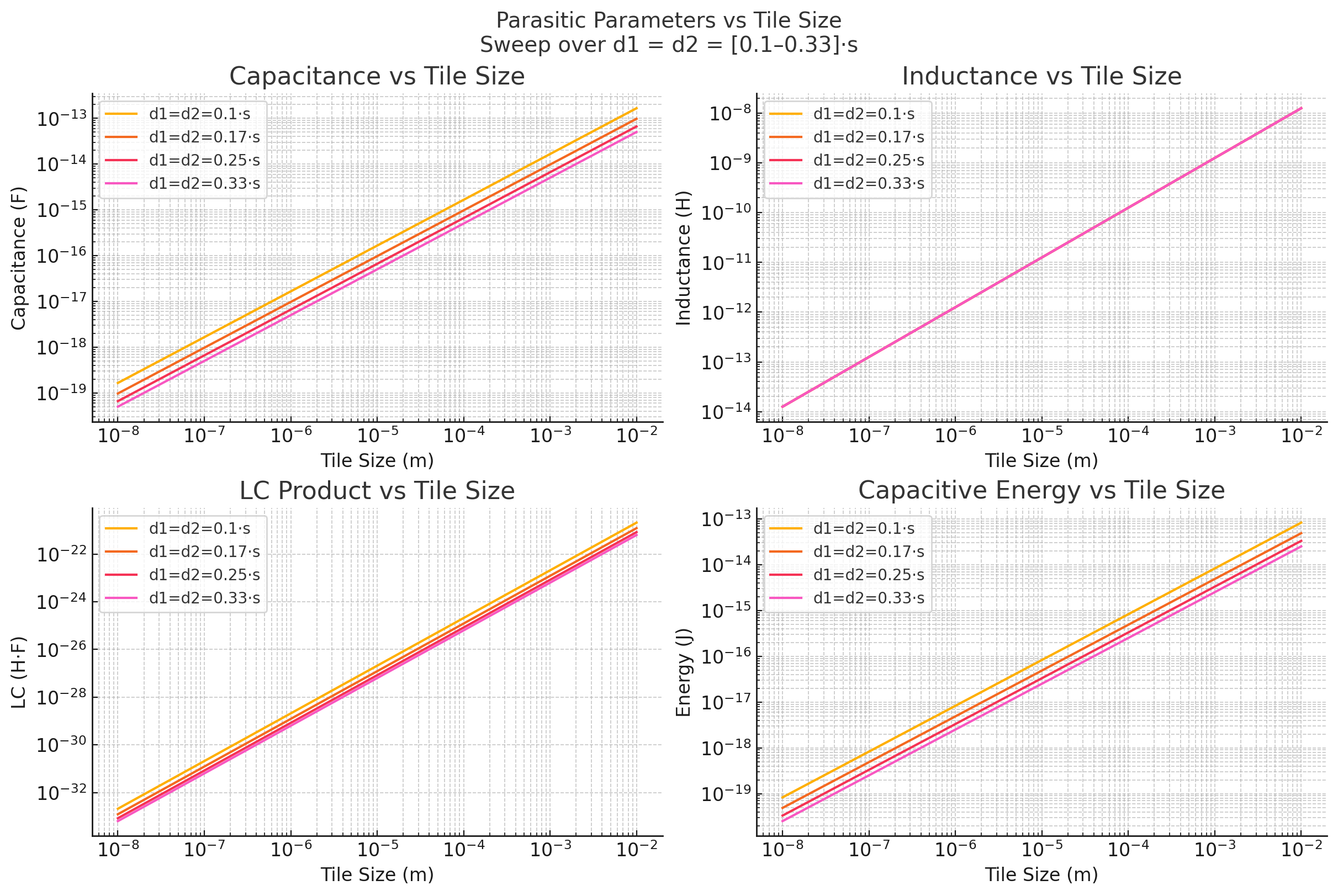
This reveals that:
Capacitance (\(C\)) decreases as dielectric thickness increases: \[C \propto \frac{1}{\frac{d_1}{\varepsilon_{r1}} + \frac{d_2}{\varepsilon_{r2}}} \propto \frac{1}{d}\] With both layers scaling proportionally to \(s\), increasing \(k\) lowers capacitance.
Inductance (\(L\)) remains unaffected: \[L \propto s\] Inductance is governed by tile geometry and is independent of dielectric spacing.
LC Product (\(LC\)) decreases: \[LC \propto C \cdot L \quad \Rightarrow \quad f_0 \propto \frac{1}{\sqrt{LC}} \uparrow\] Thicker dielectric layers lead to higher resonance frequencies.
Capacitive Switching Energy (\(E\)) also decreases: \[E = \frac{1}{2} C V^2 \quad \Rightarrow \quad E \propto \frac{1}{d}\] Lower capacitance leads to reduced energy dissipation per logic transition.
These results confirm that increasing dielectric thickness improves signal bandwidth and reduces energy consumption. However, this must be balanced against mechanical constraints and overall system height. In our 4BI implementations thus far, thickness of substrate significantly affects the complexity of circuit due to height limits of the end effector.
These models form a basis for projecting interconnect performance as tile sizes are scaled down from millimeter, to micrometer, to nanometer regimes, and future work will be done on numerical simulations and experiments to validate these analytical performance projections.