5 4BI Connector (4BIc)
4BI has clearly demonstrated its ability to be automatically assembled by an assembler and still has a lot of headroom to explore. However, joint reliability remains an issue; scaling is pointless if the approach itself is flawed.
While 4Hp was difficult to scale, its H-eon interconnects made for very reliable connections. How can we incorporate these features from 4Hp into 4BI?
The answer is 4BIc, incorporating a leadframe into the tile itself adds compliance at each joint, which evenly distributes forces and creates conductivity at reasonable forces.
While I spent most of my time on VMDs and DICE, I also spent time developing a process flow for fabrication of electrical Connectors in a Day (eCiD).
5.1 Electrical Connectors in a Day (eCiD)
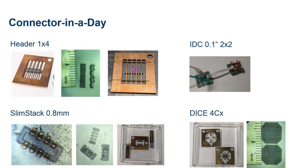
Over the past two decades, additive and subtractive desktop fabrication technologies have steadily improved in reliability and resolution, to the point where the edge of their capabilities are able to prototype electrical connectors, which may require features in the 10s of microns. Sub-$5000 desktop machines such as the Xtool F1 Ultra, Carvera CNC, and Formlabs Form 4 are able to achieve resolutions in this ballpark, and example interconnects were fabricated to explore this capability space.
| Connector Type | Fabrication Method |
|---|---|
| Header 1xn | Leadframe: Fablight, Carvera CNC |
| IDC 0.1” 2x2 | Leadframe: F1 Ultra |
| SlimStack 0.8mm | Leadframe: F1 Ultra |
| DICE 4Cx tile | Leadframe: F1 Ultra |
| H-interconnect (eye-of-the-needle) | Leadframe: Fablight |
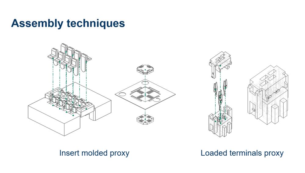
5.1.1 Assembly Techniques
Towards making connector assembly techniques more accessible, I developed several proxy approaches to approximate an insert-molded or contact loaded interconnect, shown in Figure 5.2. In some cases, the proxy was exactly the same approach as would be traditionally done, except I used digital fabrication techniques to replace conventional manufacturing methods, such as substituting an injection-molded housing with a resin printed part.
For insert molded proxies, I explored two primary techniques. The clam-shell technique involved splitting housings into two parts (part A and B), where the leadframe was mated to registration features between the two parts. After adding adhesive, I used the two parts to sandwich and seal the leadframe. This approach allowed me to achieve precision alignment without specialized molding equipment. I also investigated the print-pause technique (insert-printing), where I started an FDM print using a 0.2mm nozzle (or smaller), paused the operation to insert a leadframe, and then continued the print. This method effectively embedded the leadframe within the printed structure, creating a robust mechanical and electrical assembly.
For situations where traditional contact loading was preferred, I developed a loaded terminal proxy approach. In this process, I printed a housing instead of injection molding it, but then loaded contacts normally as would be done in conventional connector assembly. This hybrid approach maintained compatibility with existing connector designs while leveraging the accessibility of digital fabrication for the housing components.
5.1.2 Housings
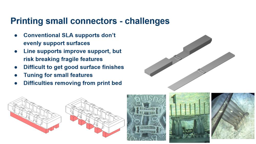
Connector housings typically rely on micromolding and operate very close to the resolution limits of desktop mSLA printers, presenting unique challenges when supporting small prints. Conventional SLA support structures fail to provide even surface support across delicate features, often resulting in inconsistent quality. While line supports offer improved structural integrity, they frequently risk damaging fragile features during removal—an issue that persisted despite implementing tapered interfaces to minimize contact area.
Surprisingly, I observed no significant performance difference between horizontal versus vertical line orientations. The printing process requires meticulous tuning for small features, as achieving good surface finishes proves exceptionally difficult, and separating delicate parts from the print bed without damage presents a persistent challenge.
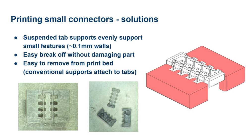
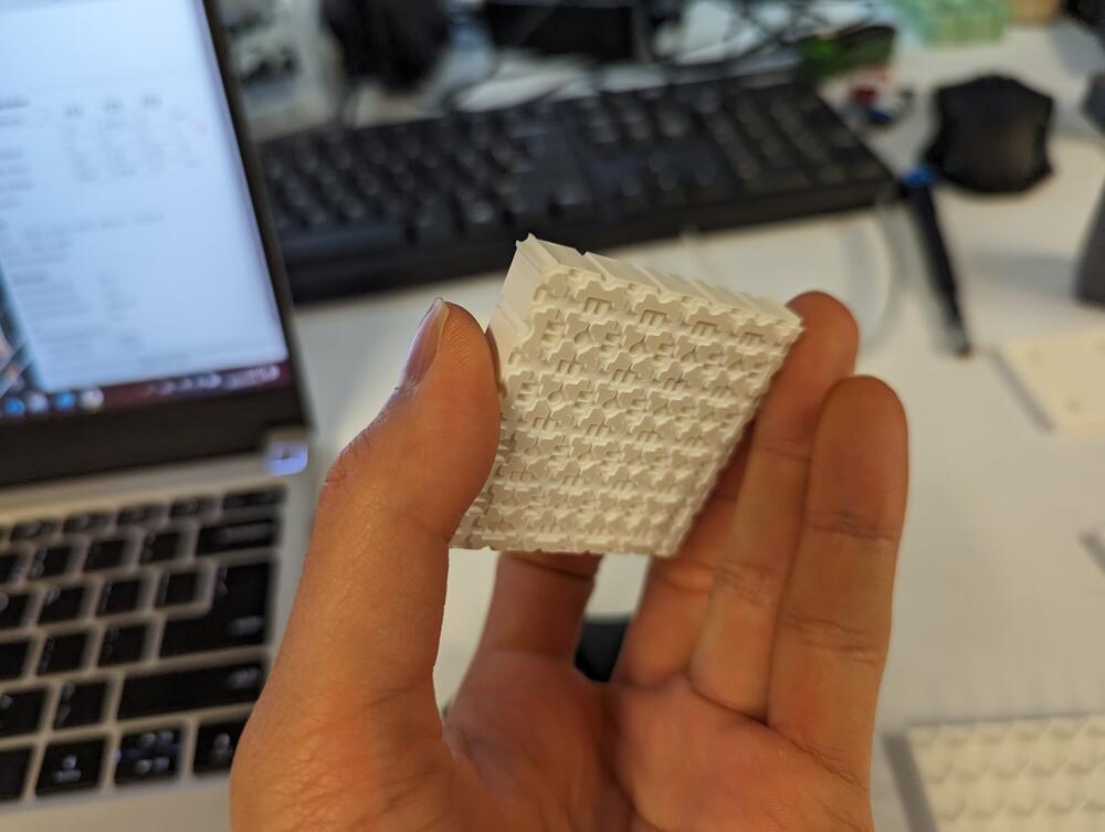
To address these limitations, I developed suspended tab supports that distribute forces evenly across small features (including walls as thin as 0.1mm), enabling clean break-off without compromising part integrity. This approach significantly simplifies print bed removal, as conventional supports now attach to these sacrificial tabs rather than directly to the functional part, providing a reliable pathway to fabricate the fine connector geometries essential to fabricating VMD geometries.
Additionally, I discovered that adding backside channels to alleviate cupping (Figure 5.4) from internal contour features makes a significant improvement to dimensional accuracy of prints.
5.1.3 Leadframes
Leadframes are usually made out of red metals (copper-based) to maximize electrical conductivity. C110 was a good starting point, but for fabricating compliant flexures, I preferred Phosphor Bronze (C510) or Brass.
In my approach, I used fiber lasers to cut leadframe positives out of stock sheet material. I worked with both the machine shop 3kW Fablight and the desktop Xtool 20W F1 Ultra, demonstrating the process at different scales. For relatively thicker metals, like 0.6mm, I preferred using the Fablight. For thinner metals, around 0.127mm, I preferred using the F1 Ultra.
My leadframe designs incorporated several standard features. I included pilot holes to register the carrier to the process. In high-volume reel-to-reel processes, these pilot holes would continuously register to the conveyer motion system, guiding materials through multiple processes progressively. This enables techniques such as progressive stamping.
I implemented tiebars to mechanically hold and support design features in place during processing. Because they needed to mechanically support design features, I found the orientation of the leadframe with respect to gravity and direction of travel was important for retaining geometry shape; lack of sufficient support easily led to deformed features. This was especially important in a high-volume reel-to-reel context; while certain designs could retain their shape at low speeds, high speeds may introduce additional forces.
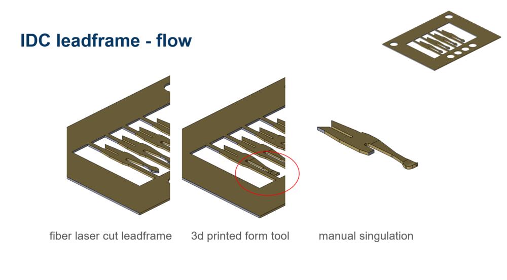
After singulation (separation of tiebars), contacts were typically the end result of my leadframe fabrication process.
For tooling, I used forming to deform leadframe contacts out of plane. This helped me accomplish many objectives, but the primary one was making sure the contact interfered with its mating target for electrical conductivity. I also explored coining, a variation on forming where a small precise feature of the metal was deformed out of plane, also useful for creating interference with a mating target. Finally, I used singulation to shear away the metal, typically for removing tiebars and isolating the contacts in a leadframe.
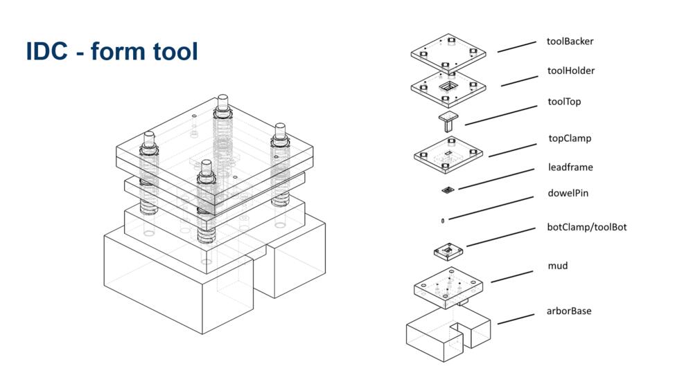
5.1.4 Process Registration
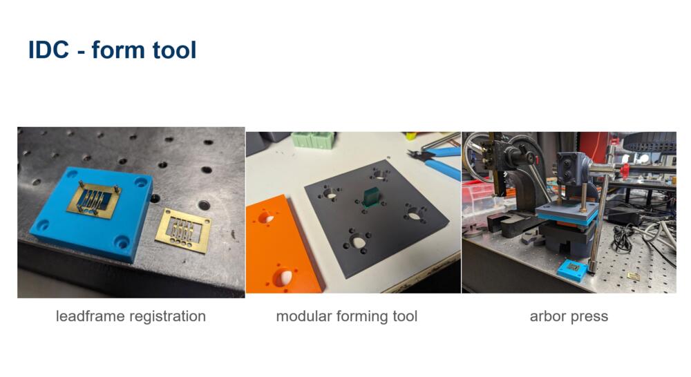
Process registration is necessary for multi-process operations where the workpiece needs to be moved from process to process. Registration is typically carried out with dowel pins, which are precision ground steel rods with tapered ends. Mating features (pilot holes) are included on leadframes.
I chose to use 2mm undersized dowel pins, which were sufficient for most designs and save on design space. They can be used in conjunction with different sized dowel pins to differentiate different purposes.
Complying with kinematic principles, 3 points of contact are sufficient for constraining a plane. 4 will overconstrain and lead to deformation of the plane.
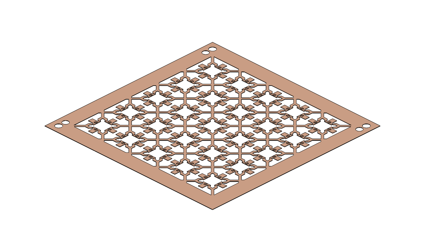
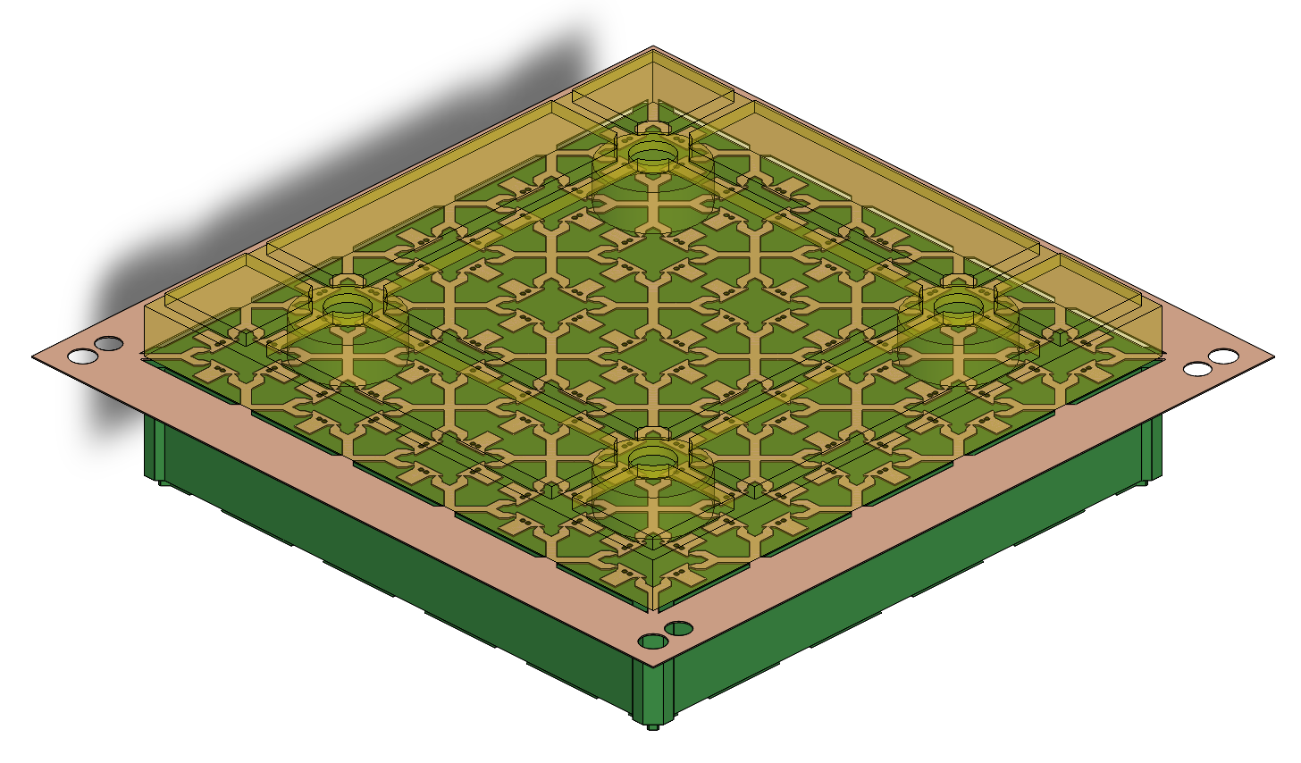
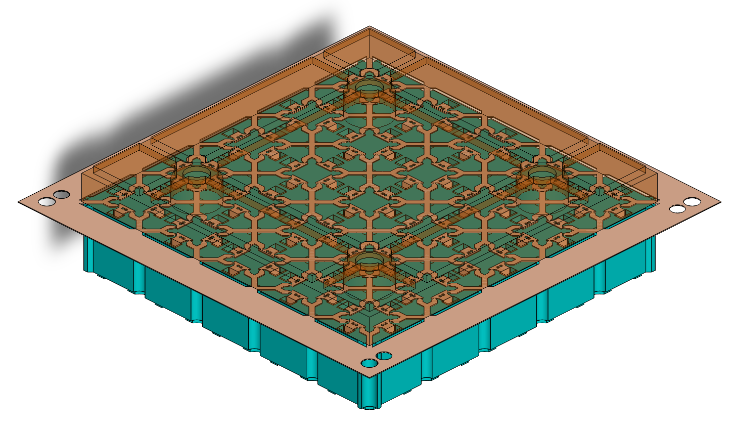
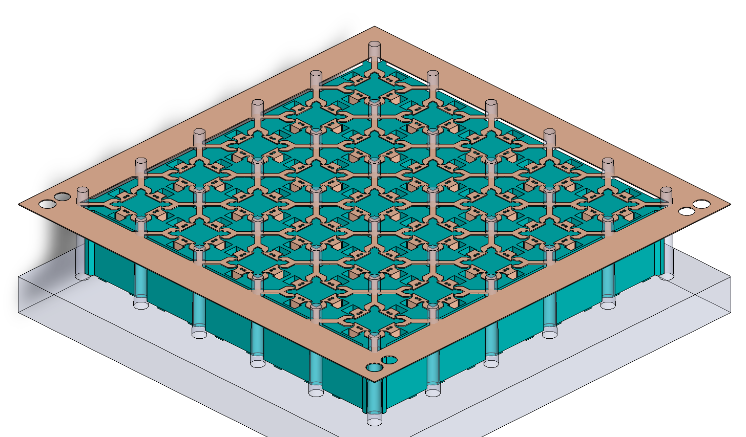
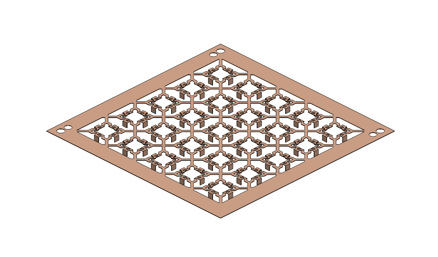
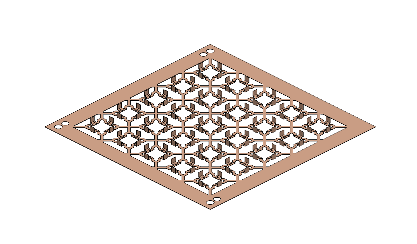
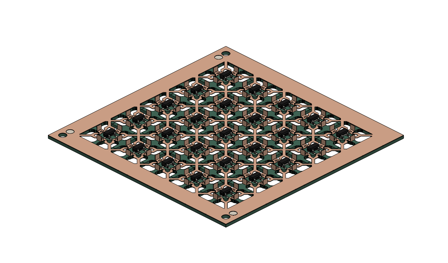
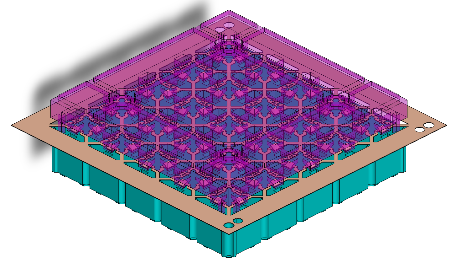
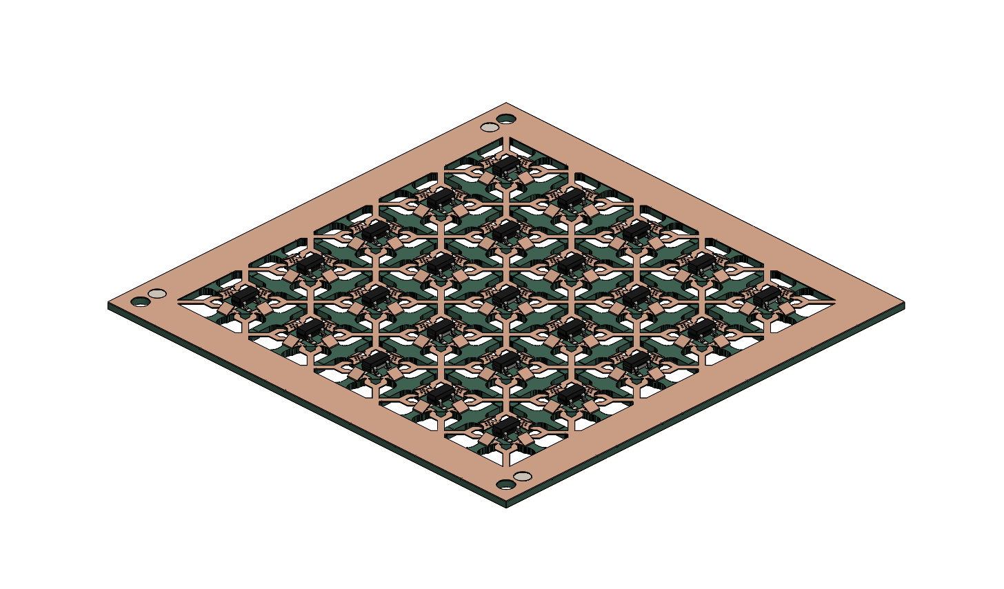
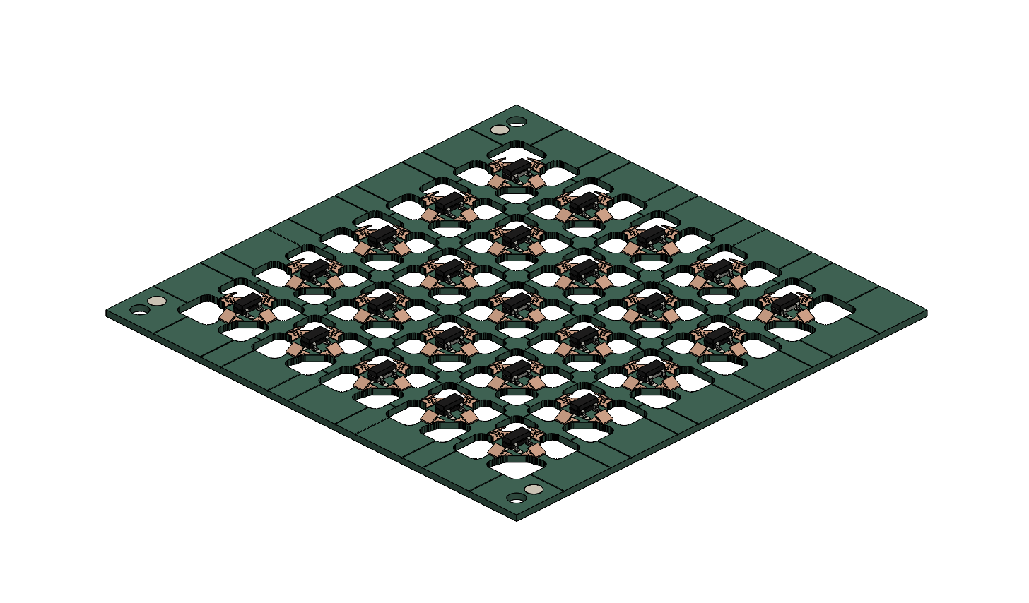
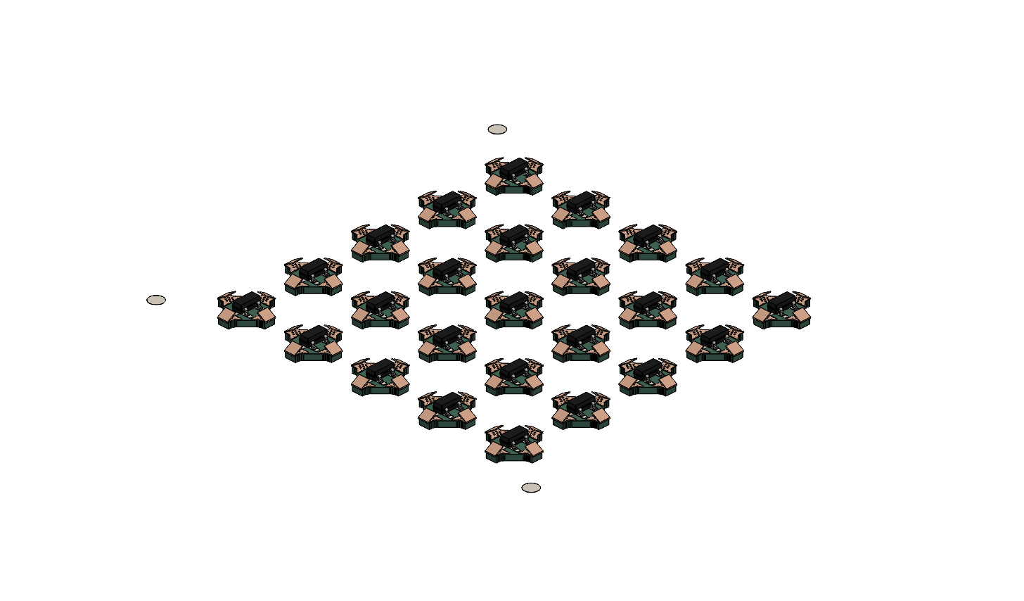
5.2 4BIc Geometry
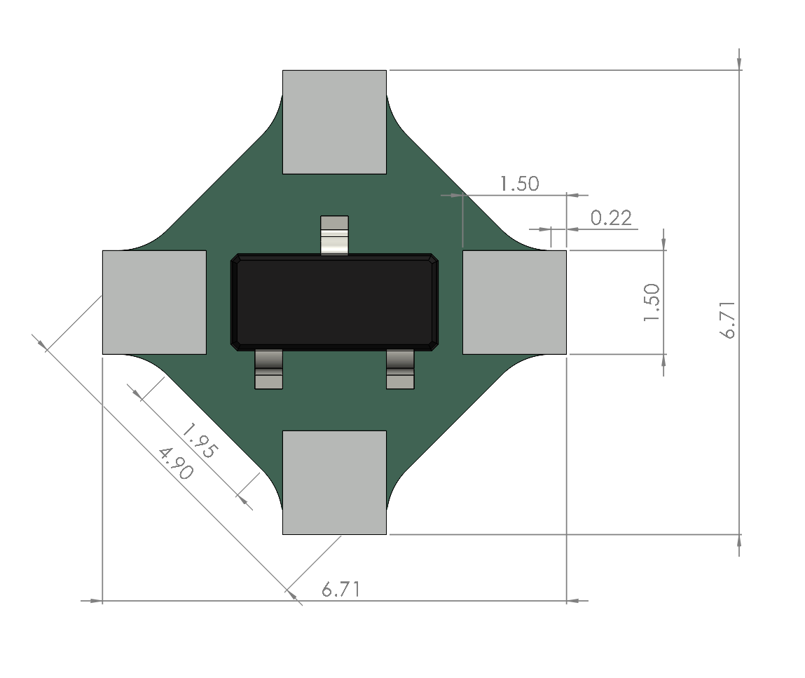
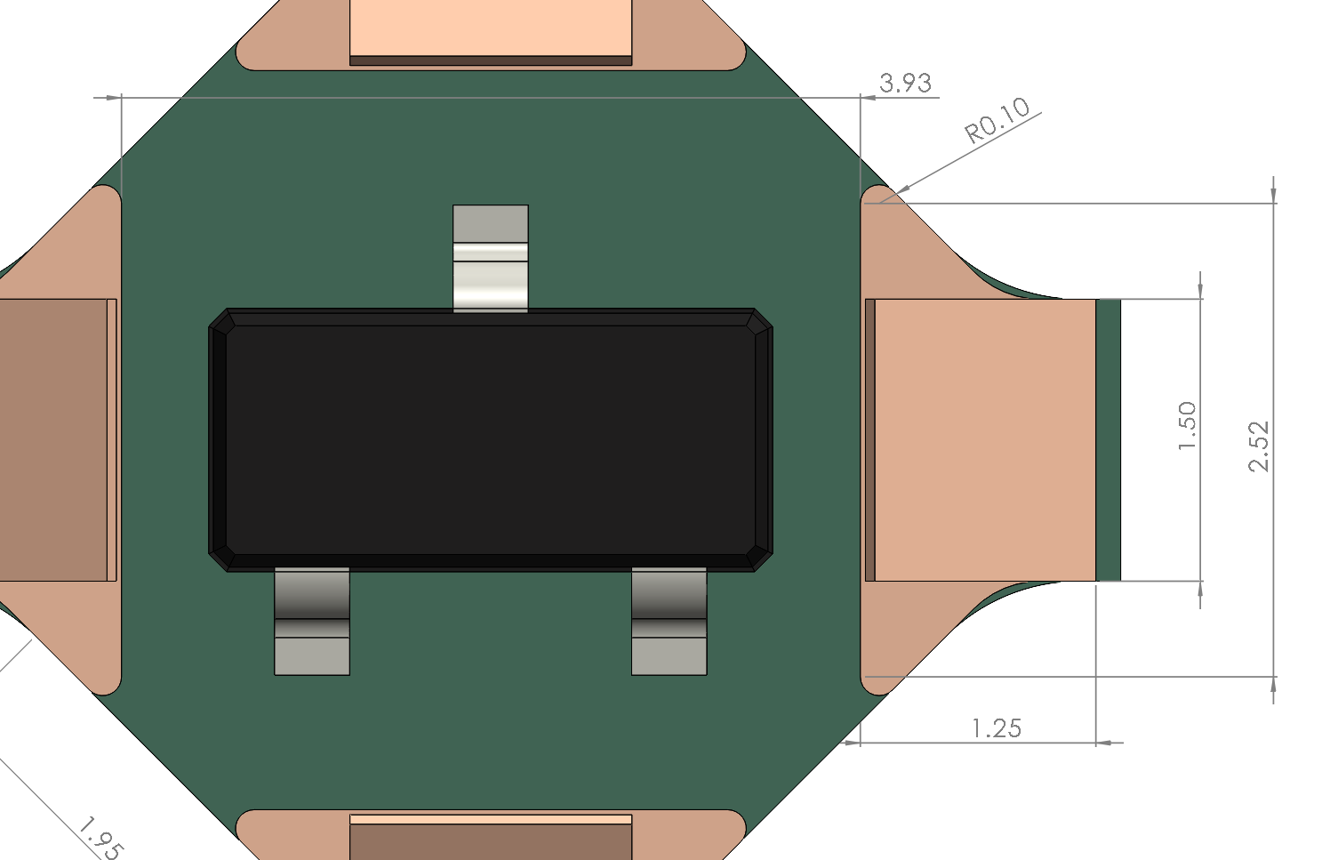
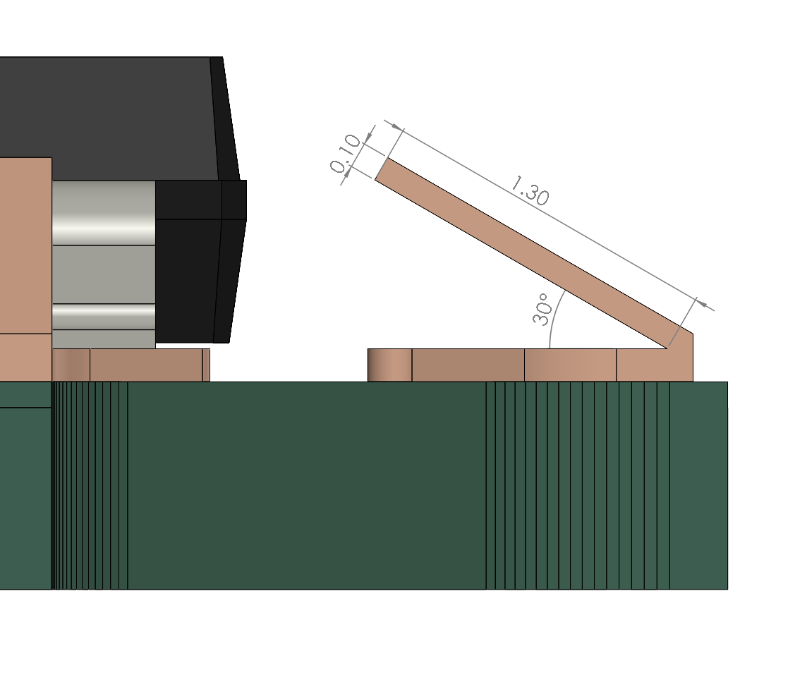
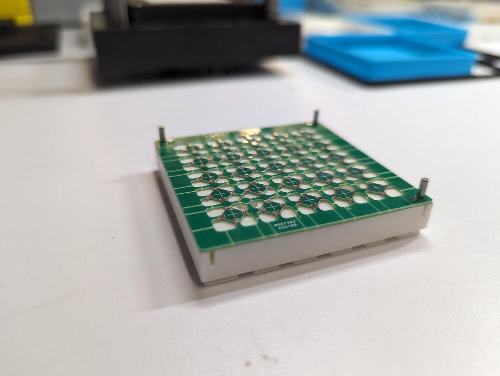
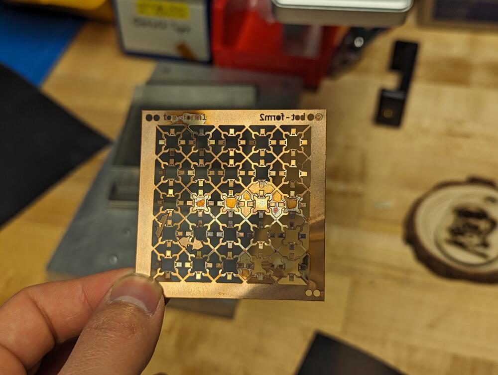
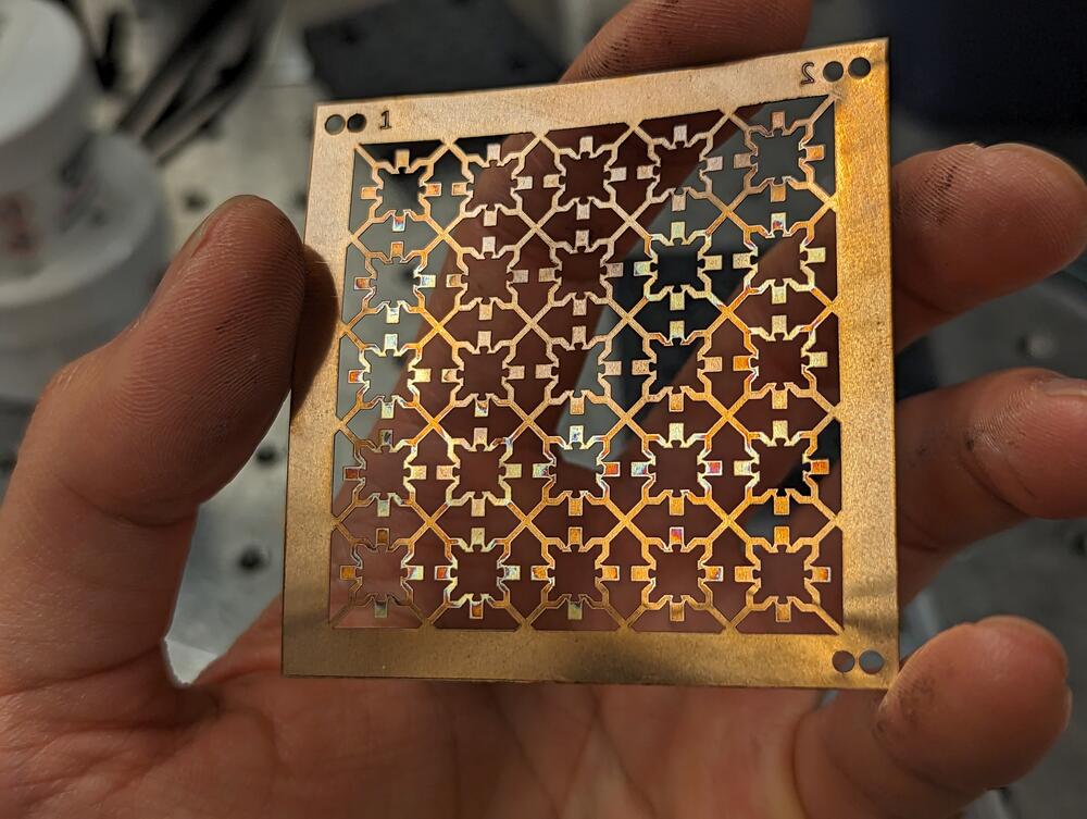
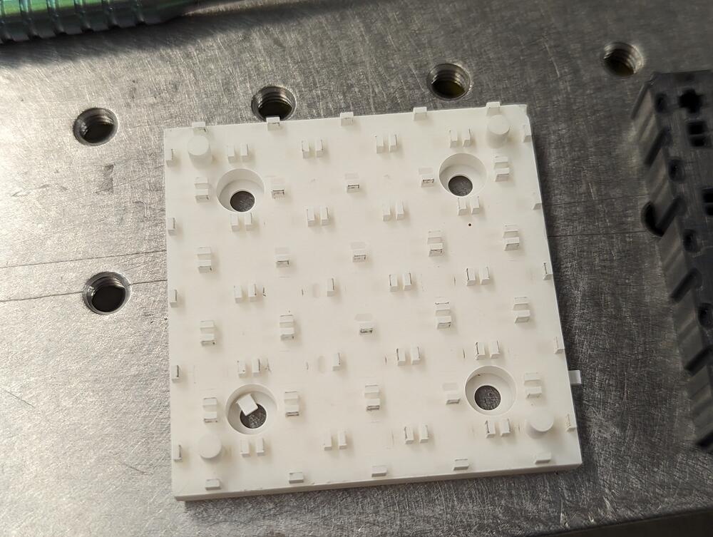
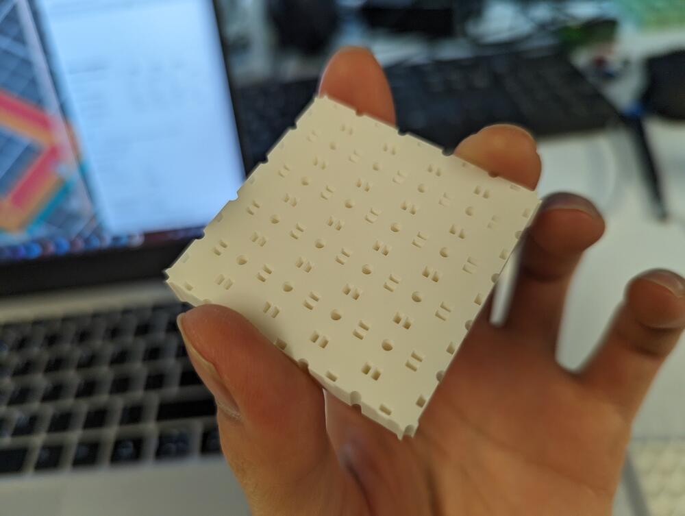
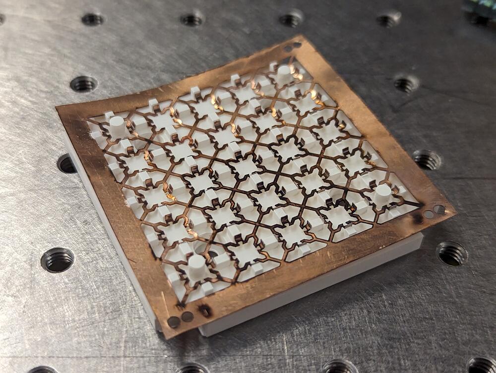
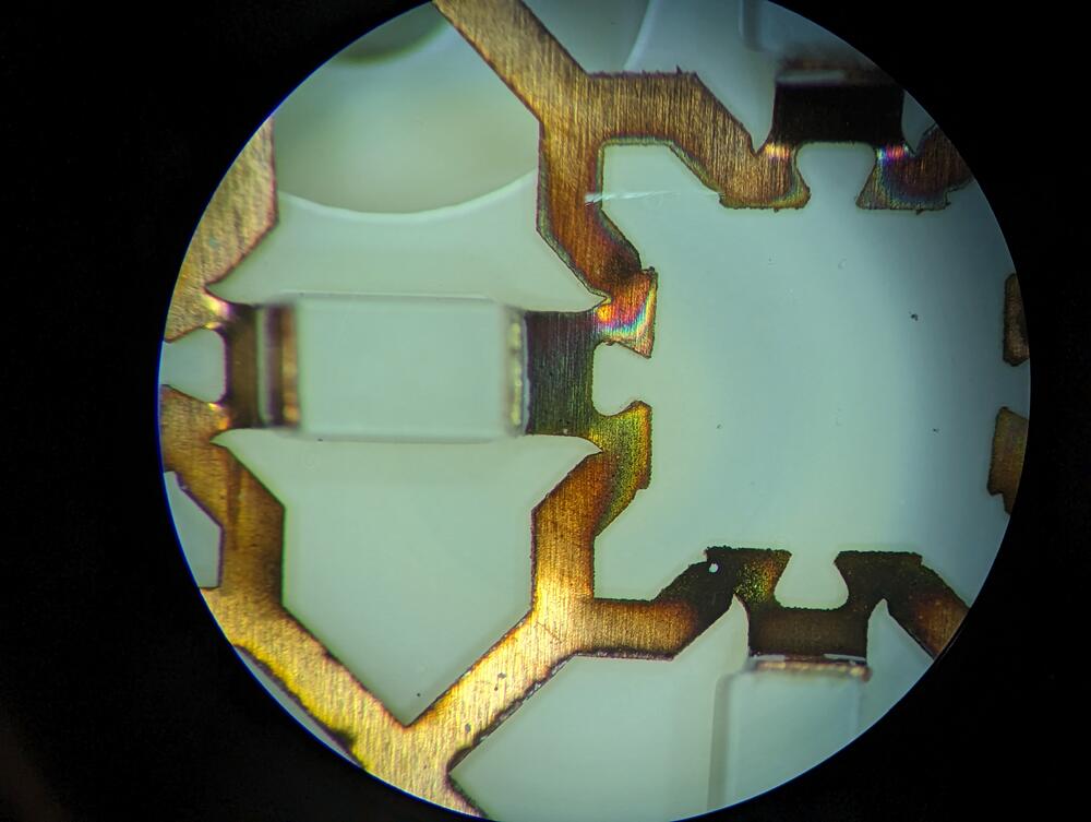
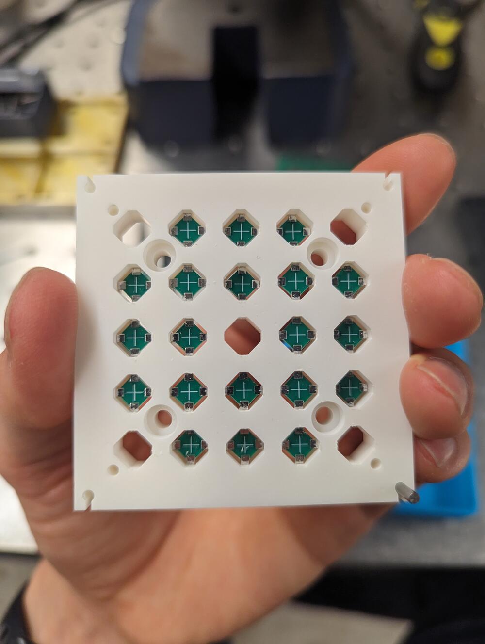
4BIc is the latest and greatest 4Bx geometry, designed for batch production to scale towards the 1000s of tiles required for bigger circuits, like the RISC-V processor on the order of 10,000s of tiles. It improves on 4BI by adding a leadframe, creating “leaf spring” compliant geometry for each contact. This approach is inspired by the leadframe principles present in connectorized electronics packaging technologies such as the ASEP technology [1]; [2]; [3].
5.2.1 4BIc Process Steps Overview

5.2.2 Panelized PCBs
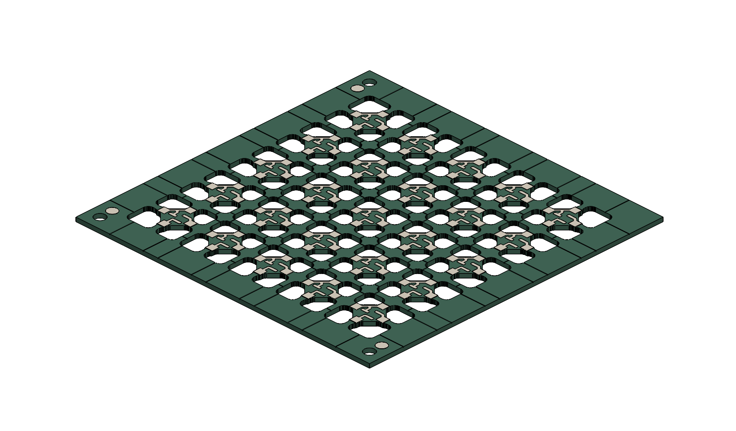
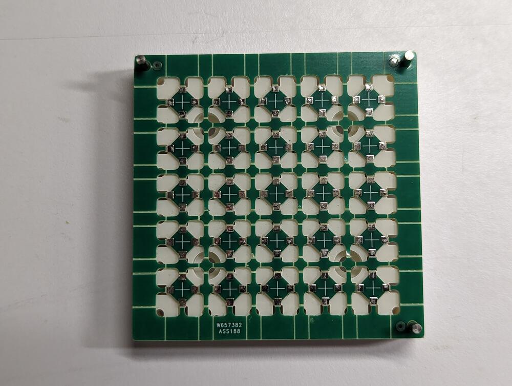
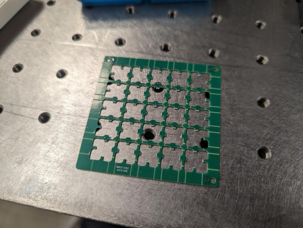
Over the course of geometry iteration, having enough tiles to test assembly and build circuits with became a bigger bottleneck than design iterations themselves. For 4BIc, it made sense to order many tiles, since it had been relatively stable as a design and we’ve made good progress on assembly with it.
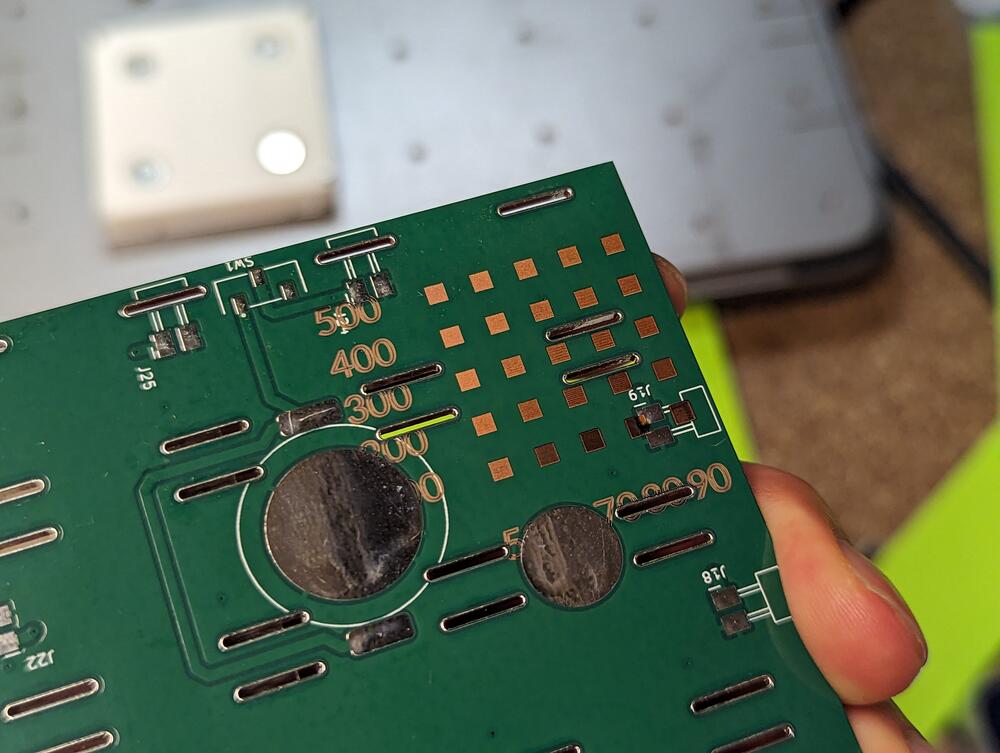
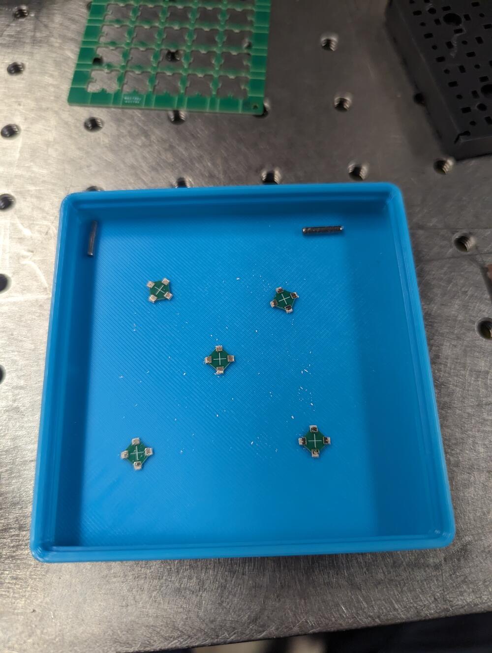
Each panel contains 5x5 = 25 tiles, and were ordered as v-cut panelized panels. This was deliberately chosen over mouse-bites due to ease of singulation by tool. In an attempt to standardize certain elements of the design, such as silkscreen patterns for visibility, both sides of the PCBs looked nearly identical. Laser marking was used to differentiate the backside from the front, conveniently a 2 second job.
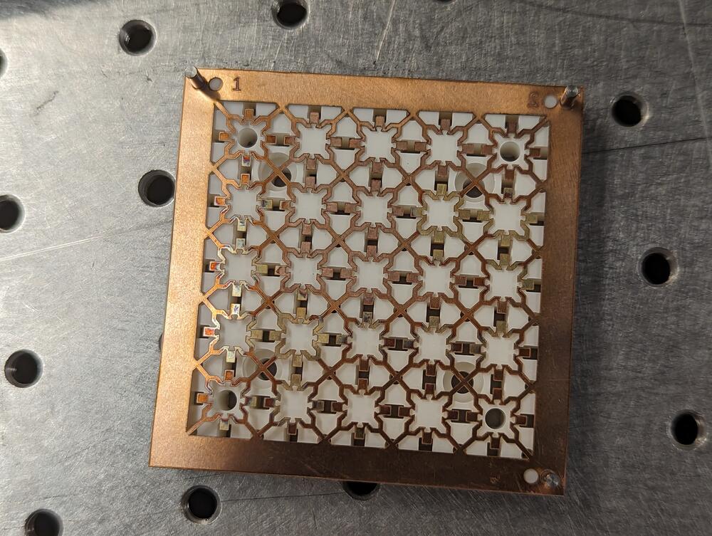
5.2.3 Leadframe Fabrication
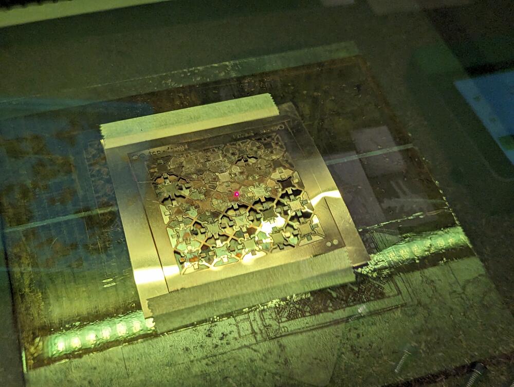
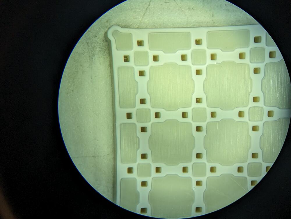
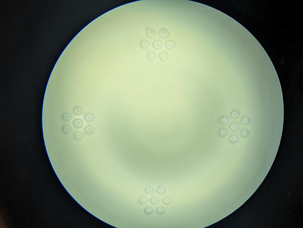
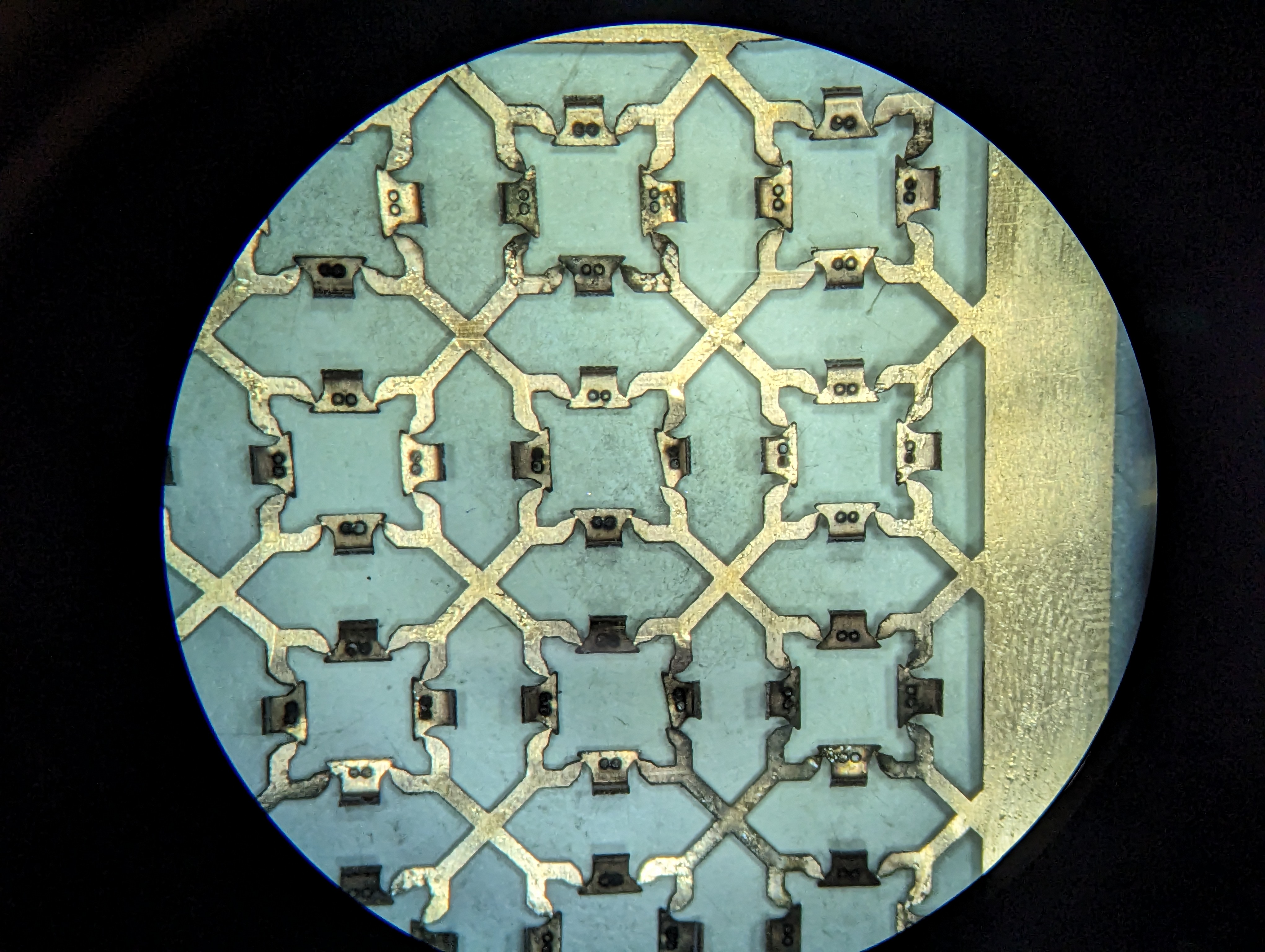
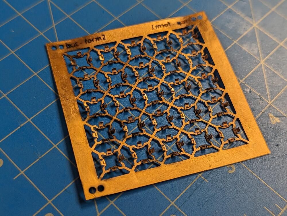
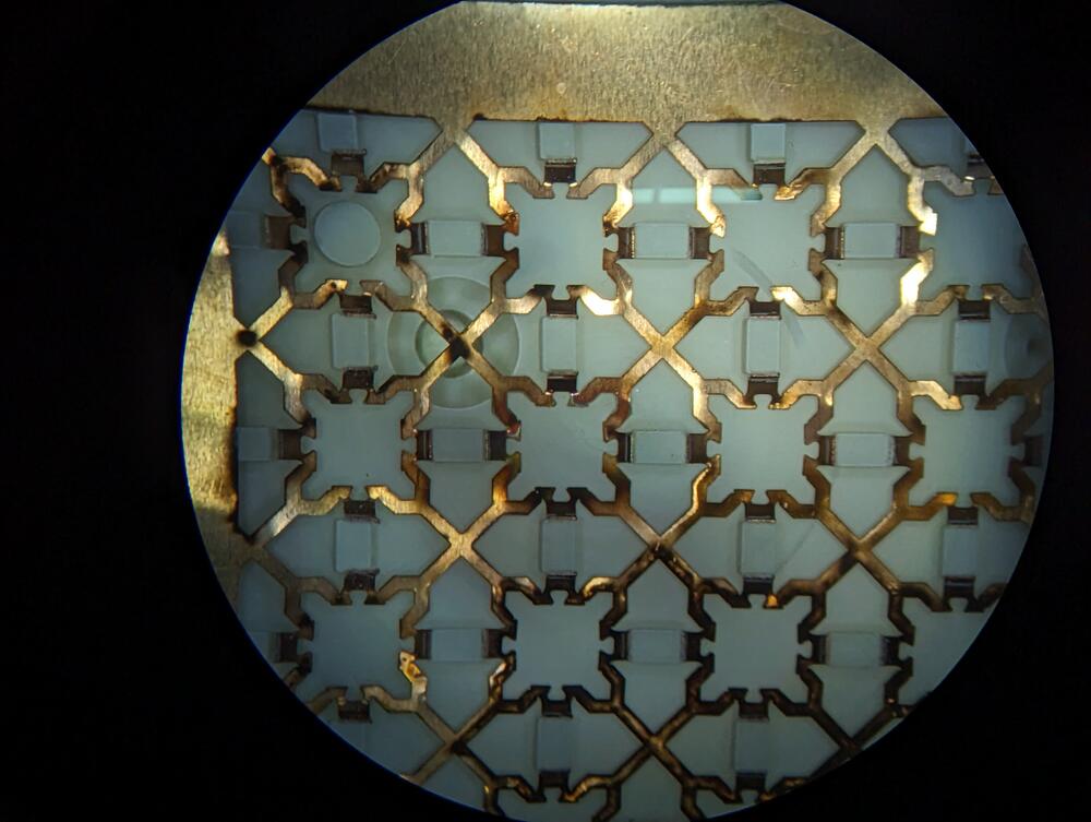
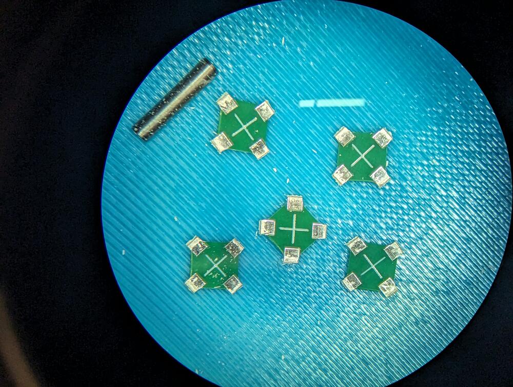
4BIc uses 0.127mm thick phosphor bronze (C510) stock for its leadframe, which takes ~4-5 minutes to cut on the F1 Ultra (Figure 5.12).
There were challenges maintaining quality of cut for leadframes, and especially when considering fabricating more at small batch production. Often, the leadframe or trash would weld itself to the steel backing, which involved scraping to remove and clean. I found polyimide backing tape was the solution to this persistent issue, significantly improving both yield and processing time.
Tape fixturing orientation proved important when dealing with significant warping, which could cause stock to lift away from the focal plane during laser processing. Through experimentation, I determined that more tape generally produced better results, particularly when strategically placed to counter material warping tendencies.
Conveniently, I discovered that 0.127mm phosphor bronze was thin enough for efficiently cutting with scissors and paper guillotines, instead of power shears. This unexpectedly simplified certain processing steps, especially for quick modifications or when separating smaller pieces from larger stock sheets.
5.2.4 Ejecting Trash
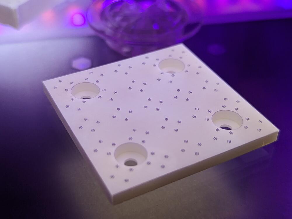
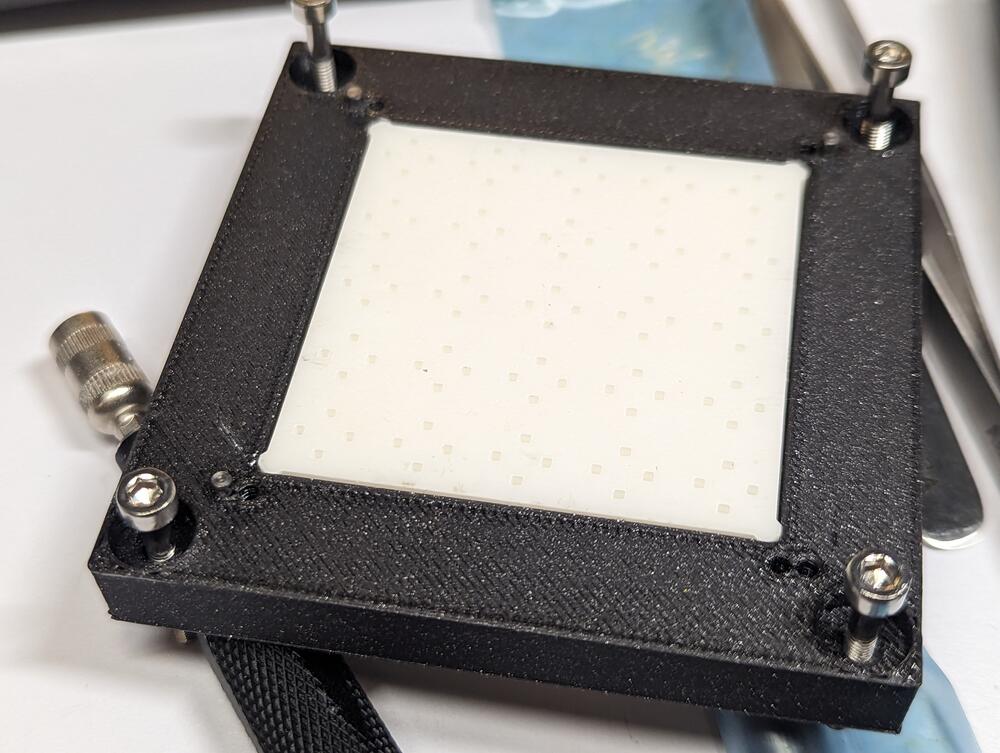
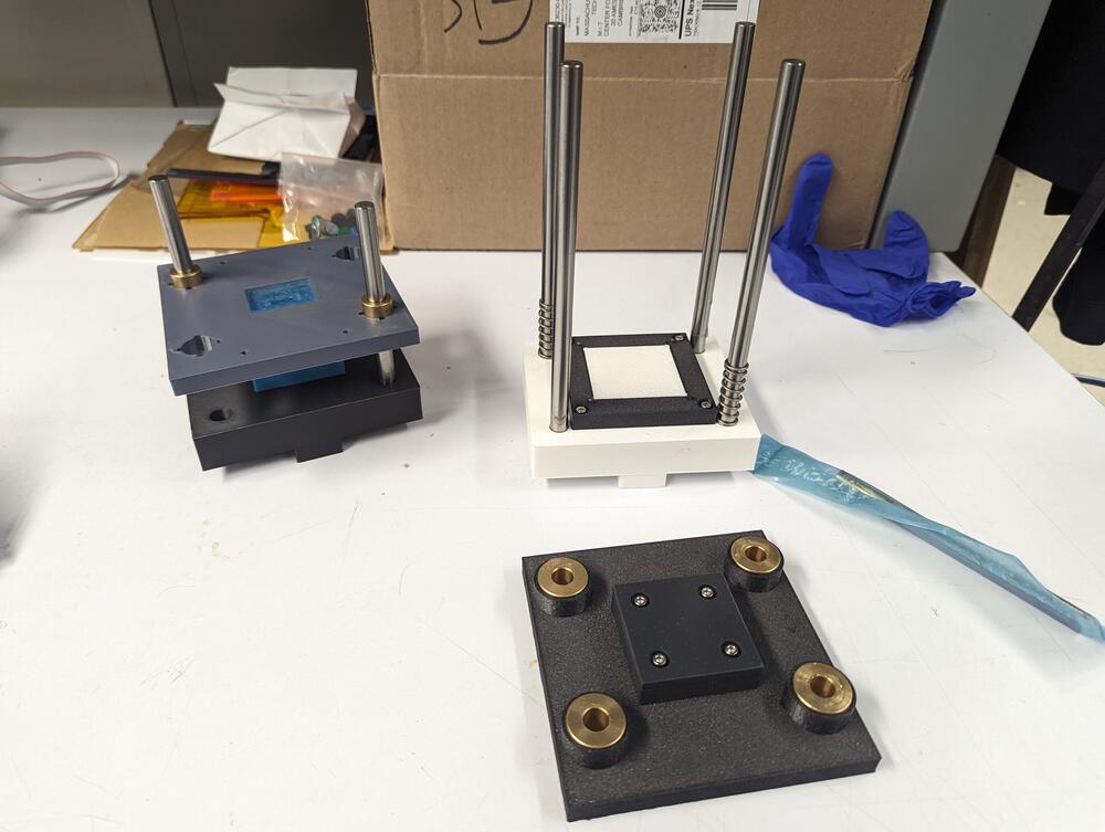
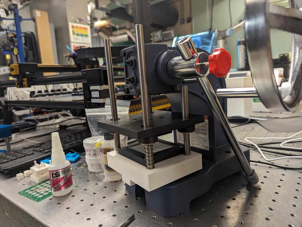
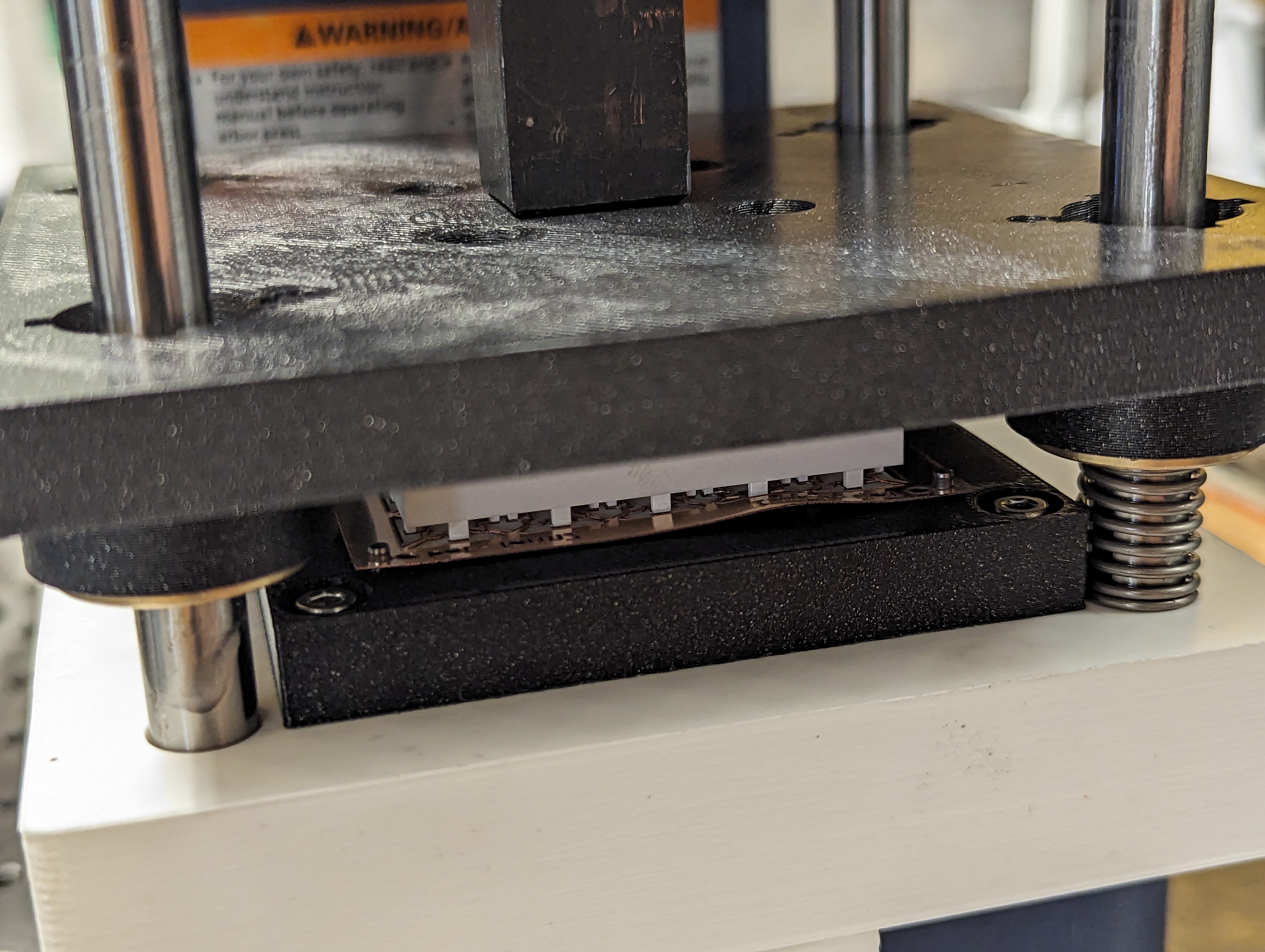
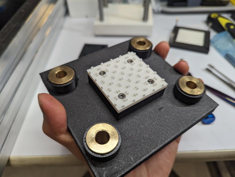
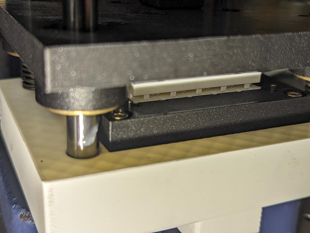
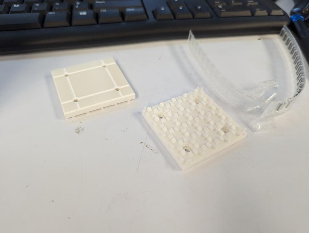
After cutting, if there are closed contour features on the inside of the pattern (such as holes), trash can get trapped. This is especially problematic if the trash is small, such as holes for solder rivets. In 4BIc, the leadframe is designed to be “married” to the PCB using a solder rivet approach, which is why ejection needs to be repeatable and comprehensive. Form 4 Rigid 10k was used to print most of the tooling, including the ejection tool initially used to remove trash.
Later, this problem was solved by reducing the number of closed countour features and merging them with larger contours, since larger trash is easier to remove.
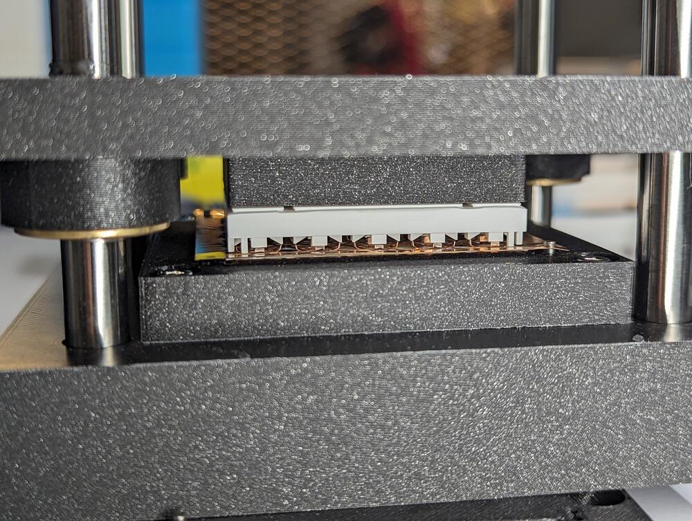
5.2.5 Form 1 Tooling for Leadframe
A lot of iteration was given to the first form (1) process. The features happened to be small enough, and the tool lacked the proper registration lead-in features that forming caused breakage in the tool. The failure mode suggested misalignment (bias to one side); the first tool lost only teeth in columns to one side.
I implemented several key improvements to address these issues. I ended up adding drafted lead-in features that engaged first to figure out alignment before the tool itself engaged, creating a self-centering effect that significantly reduced misalignment failures. Additionally, I merged the tool features together to create bigger, more robust structures, which improved durability of the tool during repeated forming operations. I also observed that the leadframe itself was twisting more than expected, primarily due to thin tie-bars, so I redesigned these elements to be thicker, effectively reducing unwanted deformation during the forming process. These modifications collectively transformed an initially unreliable forming operation into a repeatable manufacturing step essential for producing consistent leadframe geometries.
A significant feature for correctly forming parts and avoiding misalignment is adding lead-in; this feature should engage with the other half of the tool before fragile features in the tools engage. In a way, this lead-in acts like a crossing guard, making sure the two halves are aligned before crossing the street.
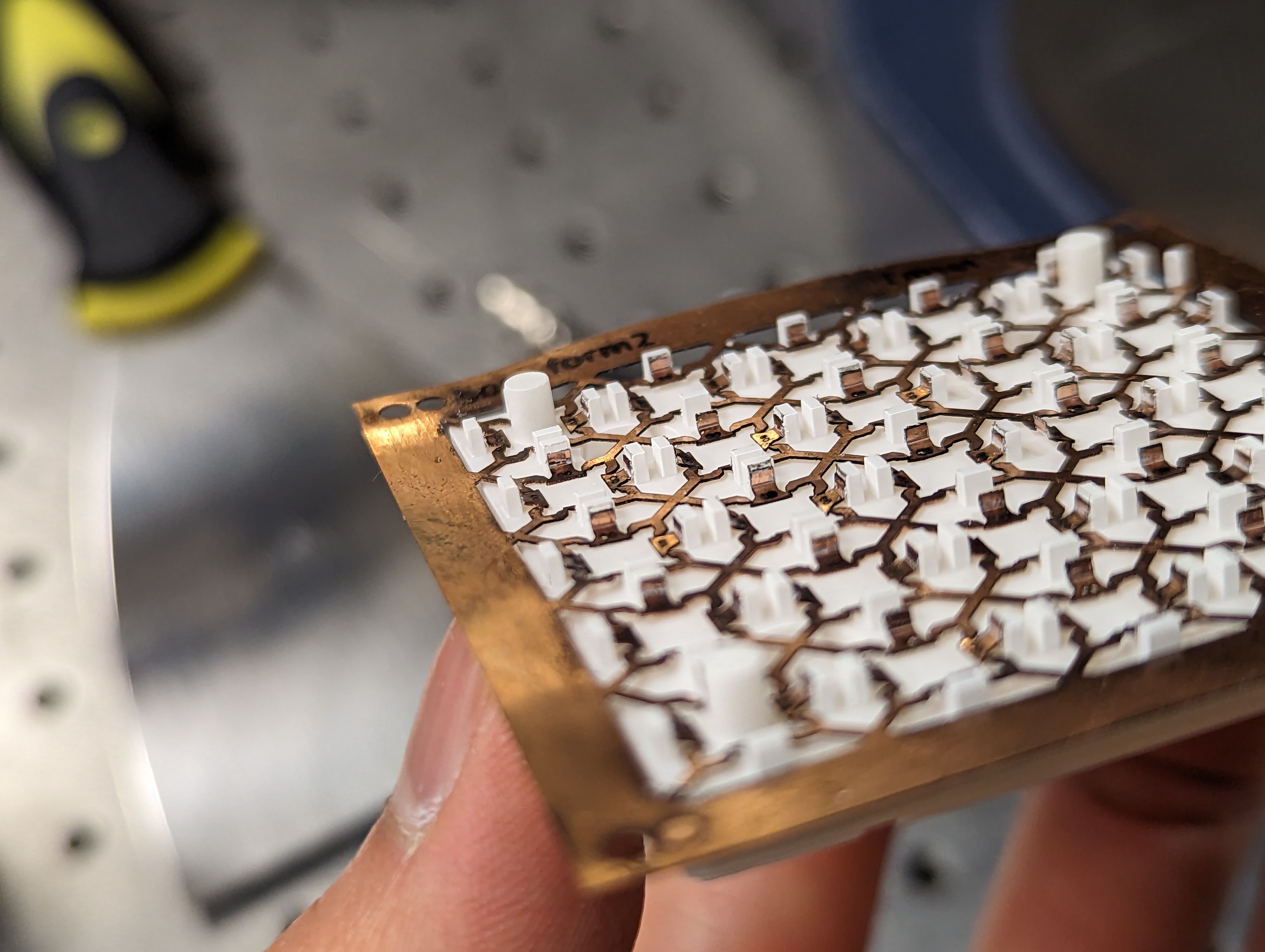
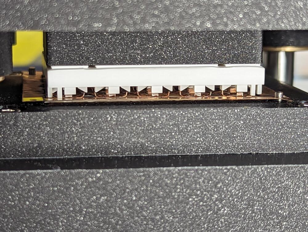
5.2.6 Formed Leadframe
As mentioned earlier, inside contour features were merged; the holes used for solder rivets were merged with the large center trash. This design modification produced several beneficial effects. The leadframe became less affected by heat, potentially causing less warping during thermal processing steps. Additionally, the trash became much easier to extract, and could be done by hand rather than requiring a specialized tool. These seemingly minor geometric adjustments significantly streamlined the manufacturing process while improving overall part quality and consistency.
5.2.7 Form 2 Tooling for Leadframe and Pcb
Unfortunately, form 1 doesn’t appear to form the contacts far enough. The form 2 operation has trouble engaging the leadframe and forming it in the right direction. Also, because form 2 has slanted features, the layer lines add roughness to the operation, which can cause binding of the fragile contacts. One solution would be to apply this form one direction at time, requiring four applications. Another solution, potentially merging the operations from form 1 and form 2 into a single step could also solve this problem; this iteration will have to be future work.
5.2.8 Tool Singulation of Pcb Panel
Although the F1 Ultra can be used to singulate FR4, it made more sense to singulate by tool. V-cut panelization typically leaves too many hairs if singulated by hand, and can be arduous (a previous timing using snippers took nearly 20min!). However, like the previous steps, a singulation tool can streamline the process, with clean and repeatable results; this tool takes up to 60 seconds to operate, if there is a jam.
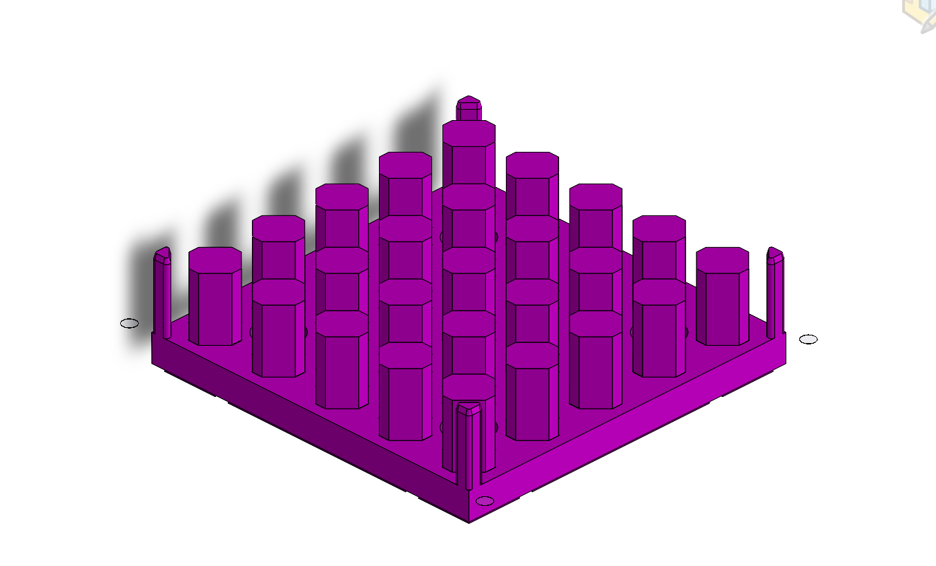
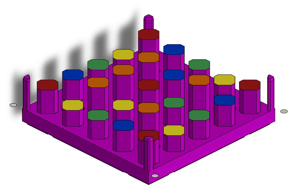
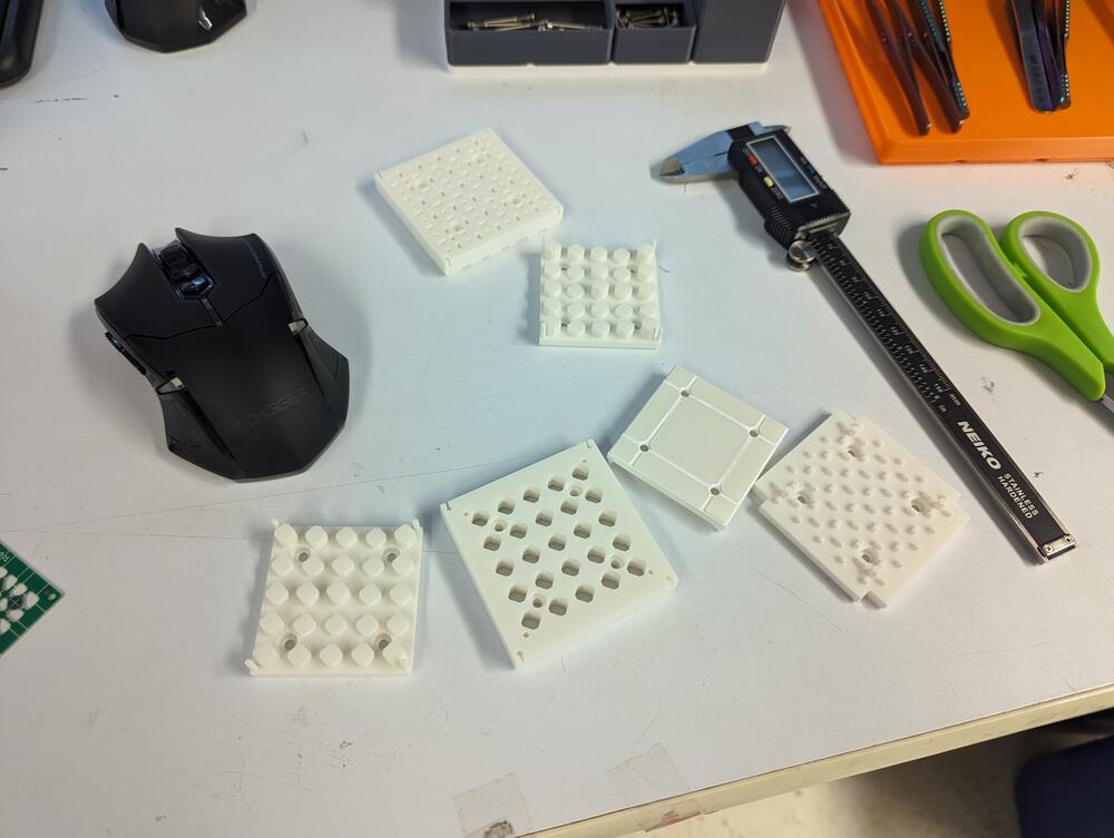
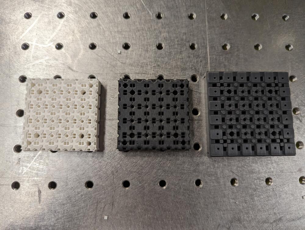
Initially, the tool was made to punch all tiles out simultaneously (Figure 5.18 (a)), upon reflection I changed the tool to progressively punch the tiles out to reduce forces (Figure 5.18 (b)). Like the other steps, there is a top (tool) half, and a bottom (clamp) half. These parts are also printed from Rigid 10k (Figure 5.18 (c)).
5.2.9 Advancing VMDs
The 4BIc geometry represents a significant advancement in the VMD ecosystem, addressing key limitations identified in previous geometries while establishing a scalable manufacturing pathway for complex circuit assembly. By integrating compliant leadframe elements directly into the tile structure, 4BIc successfully balances mechanical reliability with electrical performance – the critical challenge that constrained earlier VMD implementations.
Throughout my evaluation of joint reliability and circuit performance, I identified several persistent issues with the 4BI approach, particularly regarding intermittent electrical contacts and the high normal force window required for stable operation. Traditional pad-to-pad connections proved vulnerable to mechanical shock, vibration, and inconsistent pressure distribution, which became increasingly problematic when scaling to larger circuit assemblies. 4BIc directly addresses these challenges by incorporating leaf-spring contacts that provide consistent, reliable electrical connections at significantly lower activation forces while accommodating minor misalignments.
The manufacturing process I developed for 4BIc, though still evolving, demonstrates a viable path toward high-volume production. My stepwise approach – from panelized PCB fabrication through leadframe cutting, forming, and singulation – is deliberately designed to leverage accessible digital fabrication technologies while maintaining compatibility with established electronics manufacturing techniques. This hybrid strategy allows 4BIc to serve as a transitional technology that can be implemented immediately with today’s tools while demonstrating the architectural principles that will define future VMD systems.
Looking forward, several improvements to the 4BIc implementation could yield significant benefits. Integrating form 1 and form 2 operations into a single step would streamline manufacturing, while further refinement of the leadframe design could improve compliance characteristics. Experimenting with alternative plating finishes for the contact surfaces may reduce contact resistance even further, potentially enabling higher-frequency applications. Most importantly, now that the assembly system and manufacturing process have been established, extensive reliability testing of completed 4BIc circuits will provide crucial data for optimizing future designs.
By addressing the fundamental reliability challenges identified in earlier VMD geometries, 4BIc paves the way for scaling beyond simple proof-of-concept circuits to the larger, more complex assemblies required for meaningful computational applications. The completed RISC-V processor envisioned in this work, requiring tens of thousands of tiles, now stands as an achievable milestone on the path toward truly volumetric electronics packaging.