6 Conclusion
This thesis introduces the volume mount device (VMD) as an alternative to surface-mount device (SMD) standards, reimagining electronic packaging for true three-dimensional assembly rather than conventional two-dimensional integration.
The VMD framework embeds electrical function and mechanical structure within modular elements that form self-constraining 3D lattices. While currently incorporating SMD components on tile PCBs, this approach establishes a pathway toward eventually replacing SMDs at the IC packaging level.
My hybrid assembly system advances beyond prior work by placing hundreds of integrated elements at ~1000 CPH, compared to previous systems limited to tens of components at slower rates.
My evaluation of geometric configurations, performance overheads, and self-aligning connector interfaces establishes VMD as a viable approach for rapid electronics prototyping. Beyond simply replacing breadboards and prototype PCBs, this work lays the foundation for a scalable, reversible, and reconfigurable packaging framework inspired by natural ecosystems’ circularity. The VMD approach offers a compelling path toward more sustainable electronics systems that can be assembled, disassembled, and reassembled as needed—reducing waste while improving resilience against supply chain disruptions.
As electronics continue to evolve, the volumetric integration method demonstrated in this thesis provides a promising direction for overcoming the limitations of planar manufacturing while leveraging existing supply chains in new, more flexible ways.
6.1 Future Work
Having demonstrated an automated system capable of assembling 100s of integrated electronic digital materials, there are a few next steps that can be undertaken.
6.1.1 Finishing 4BIc
4BIc is a few steps away from being finished, but was not finished in time for this thesis. The leadframe tooling is almost there, and a new approach may consolidate multiple form steps into one, simplifying asssembly and increasing reliability. Considering the results from the full-adder evaluation, improving joint reliability is a top priority. Multiple solutions have been suggested towards evenly distributing forces between contacts, such as adding a compliant conformal layer to the cap itself, but adding compliant contacts to each pad theoretically remains the best solution that not only guarantees even distribution of force between the cap and the assembly, but predictable forces throughout the entire volume. This solution also remains the most scalable, with ample headroom for reaching higher orders of magnitude.
Joint evaluation tests will also have to be conducted on 4BIc, such as Normal Force Window and cycling tests. In addition, to validate our analytical models, numerical and experimental work will need to be done to characterize capacitive and inductive parasitics, for evaluating switching frequency as feature sizes shrink.
Breaking out connections using solder joints and pyralux was a source of error; it partially relieved strain from wires directly soldered to tiles, but could be improved (experimenting with thinner wires with less strain, applying principles from 4BIc and connector fabrication to create compliant test probes, etc.).
6.1.2 Assembly Improvements
Several improvements could immediately enhance the assembly process. For example, close-looped feeding would enable the system to effectively recycle tiles without manual intervention, reducing operator workload for large-scale assemblies. Scaling to larger assemblies will necessitate this feature; disassembly will become more costly than assembly itself.
Kinematic fixtures would reduce the need for recalibration moving feeders and templates on and off the assembler bed, saving a significant amount of time.
Additional computer vision could be used to add additional error checks, reducing the need for manual intervention and improving overall system reliability. For gathering longer term reliability data, it may start making sense adding additional cameras monitoring other aspects of the assembly process.
6.1.3 Geometric Exploration for Enhanced Reliability
While square geometries provide compatibility with existing supply chains and sufficient I/O capabilities, future work should explore alternative geometric configurations that enhance mechanical reliability. Although triangular elements offer superior kinematic stability with their three points of contact, they present challenges for electronic routing due to limited I/O capacity.
A promising research direction would be hybrid geometries that combine triangular mechanical contact points with square or hexagonal electrical interfaces. This approach could yield self-aligning structures with guaranteed contact between mechanically independent elements while maintaining adequate routing capabilities for power, ground, data, and clock signals.
Additionally, exploring true 3D elements (beyond stacked 2D elements) could unlock unique advantages in tessellation and self-orientation behavior, though this would require addressing the additional fabrication complexity outside the current manufacturing mainstream.
6.1.4 4Cx Family - 4C, 4Ci, 4Ce, 4Cs
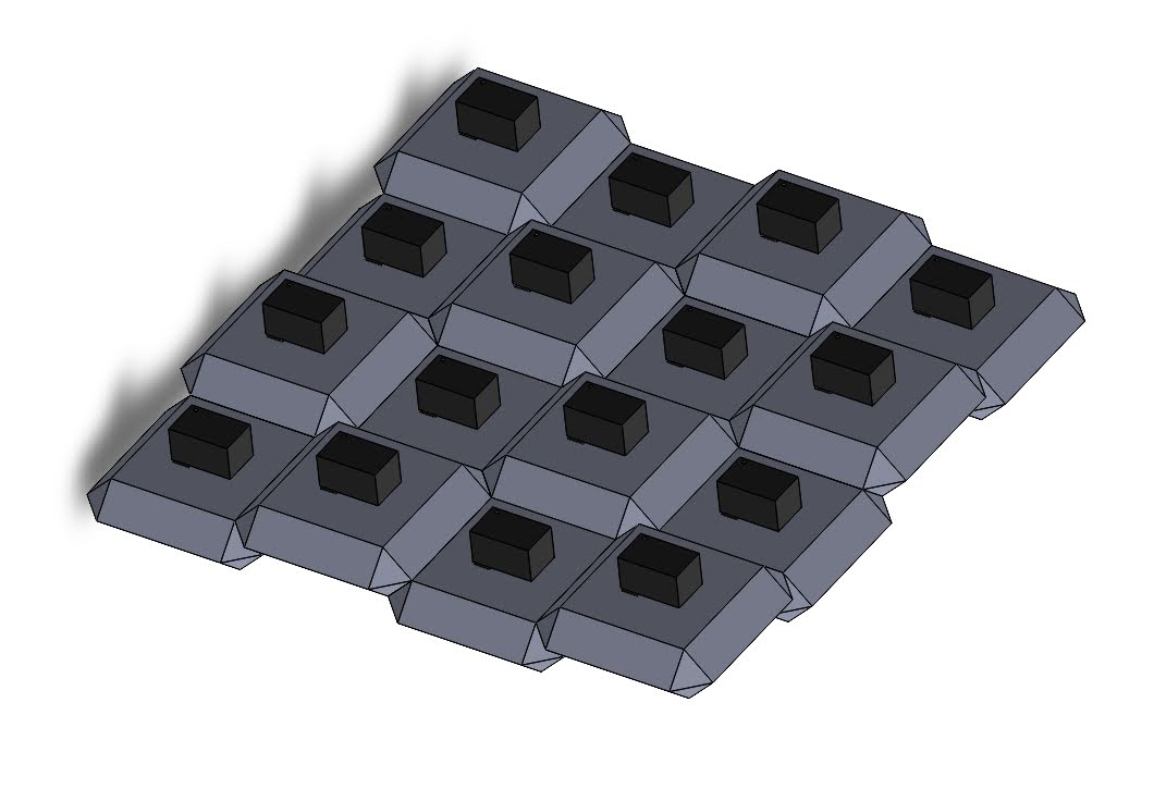
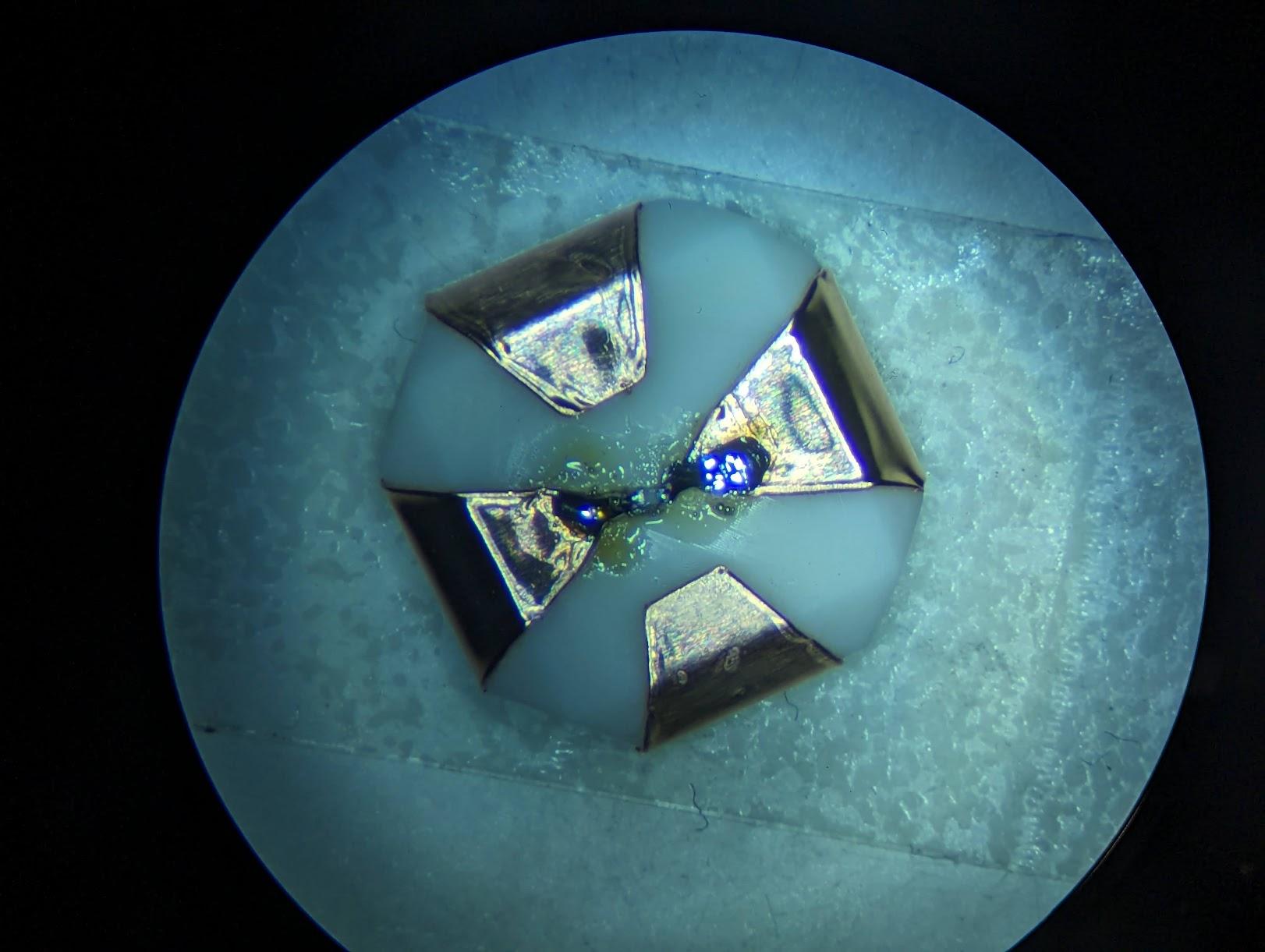
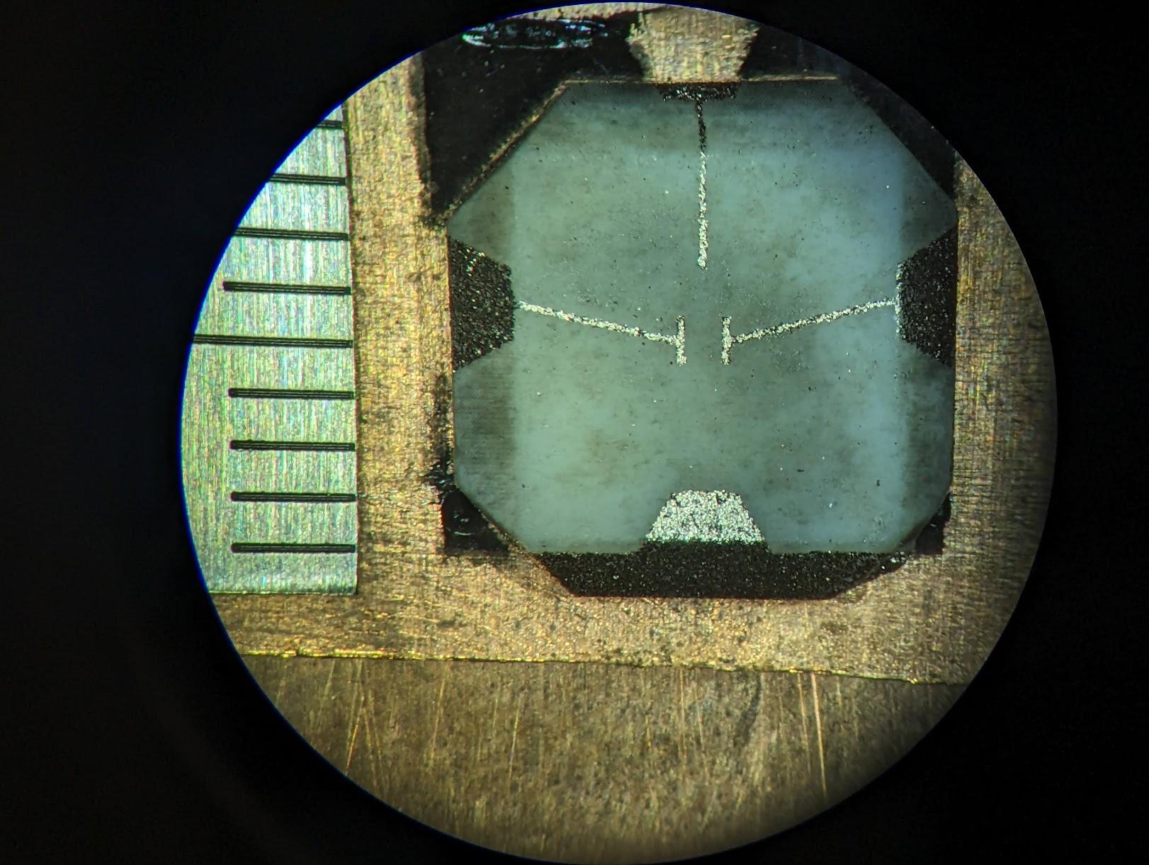
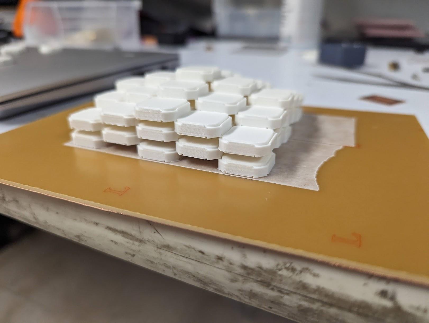
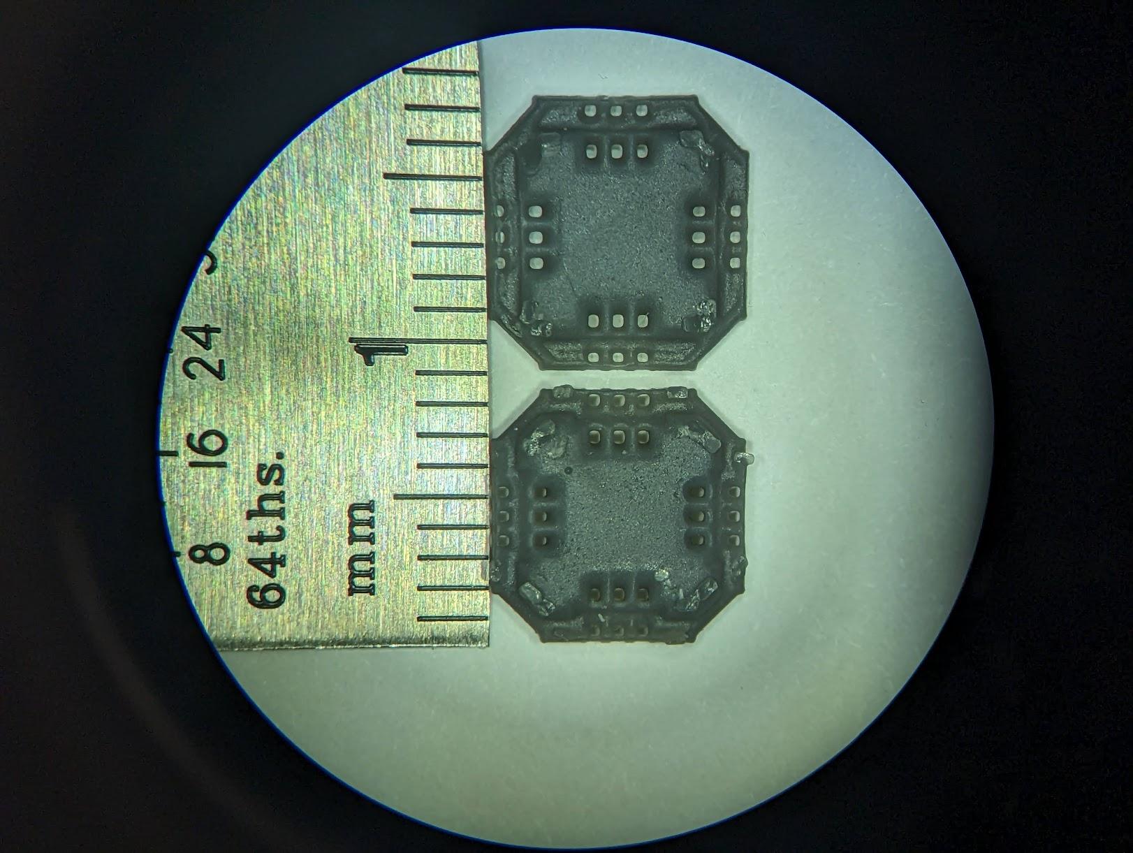
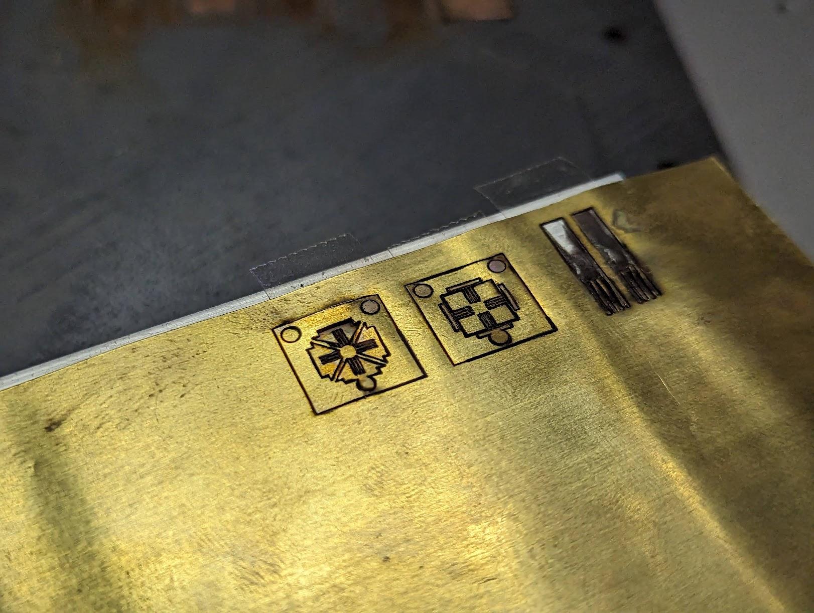
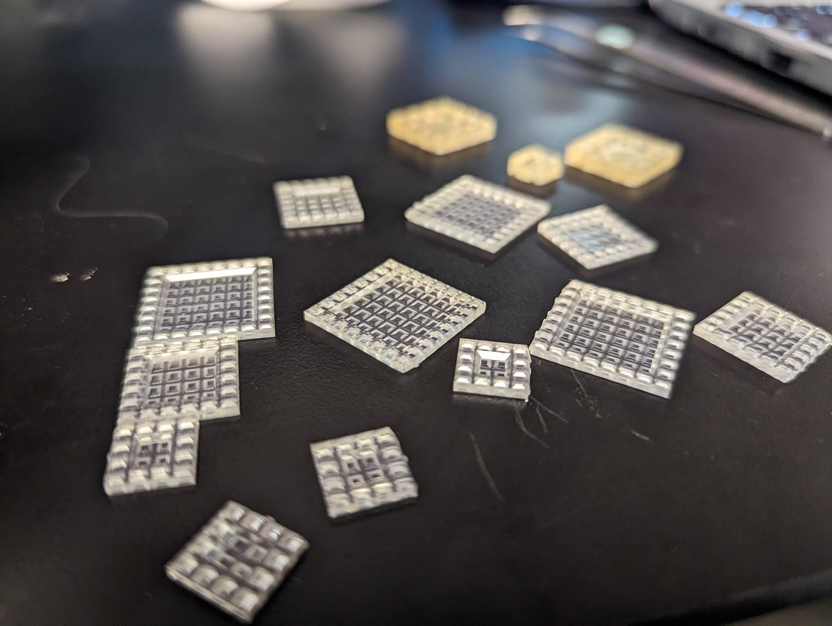
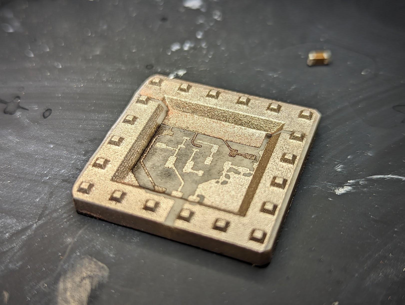
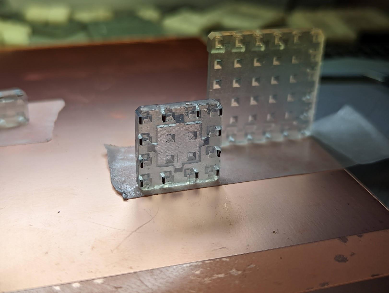
In addition to 4Bx work, efforts were made towards exploring more self-aligning geometries in the 4Cx (connector1) family, which are also capable of handling higher pin count and higher power necessary for application goals such as variable-pin chiplets and power electronics, shown in Figure 6.1.
Initial work on 4C relied on chamfered edges mating flush with adjacent tiles. However, the design of these edges only constrained the tiles in height, and not laterally in xy. 4Ce (edge) introduced “kinematic” french-cleat like designs inspired by Jake Read’s “Kleat Toolchanger” mechanism from his Clank machines project [1]. My implementation in geometry enabled constraint in both height and xy, but created failure modes where the edge could act as a pivot point, destabilizing the structure when subject to external forces. Finally, 4Cs (surface) introduced aligning pillars inspired by 4BI, but directly on the surface of the tiles.
In these approaches, devices are integrated directly into the tile rather than sit on the surface, simplifying the pick and place problem for arbitrary devices of variable pin count.
These approaches represent experiments towards shifting the geometry feedstock itself away from conventional 2d approaches, such as PCBs, towards more 3d approaches, closer to Molded Interconnect Devices (MIDs) [2] and ASEP [3]; [4]; [5].
6.1.5 uVMDs and nVMDs
While this thesis focuses primarily on scaling element count using millimeter-scale components to enable sophisticated circuits, a parallel and complementary trajectory involves scaling down feature sizes from millimeter to micrometer regimes. This miniaturization approach not only allows more elements to fit within a given volume but also significantly reduces performance overhead and parasitic effects.
My colleague Teddy Hsieh from the Niroui Group is currently fabricating nano and micro devices using discrete feedstock such as 55nm gold nanoparticles, building upon Spencer Zhu’s foundational work in this area. Their research group has established a strong track record in pushing the boundaries of nanoscale engineering [6] [7] [8]. Our collaborative roadmap aims to bridge the hierarchical assembly and automation techniques developed in this thesis with Teddy’s device fabrication expertise, creating a unified approach that spans from nano to macro scales.
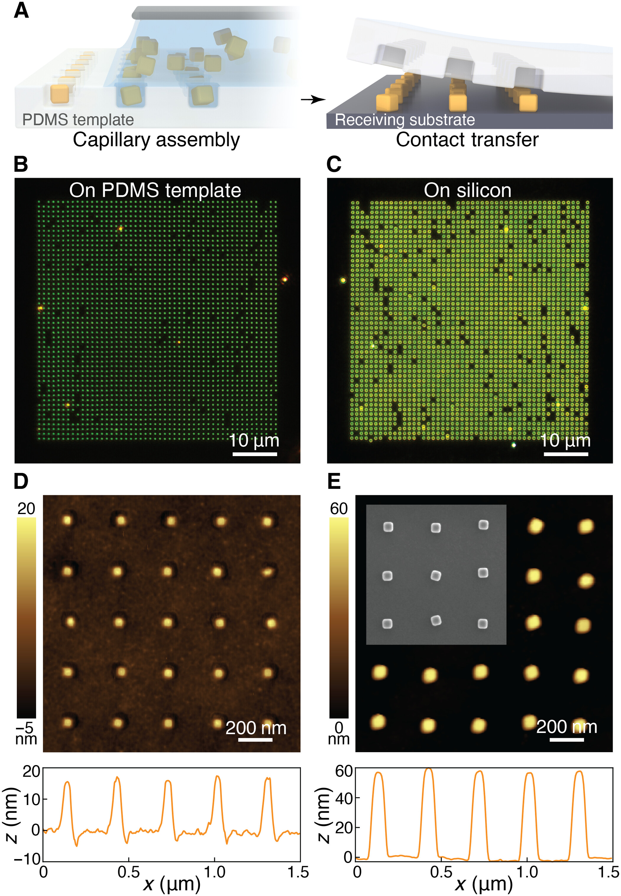
Accessing these smaller regimes requires specialized fabrication tools. The UpNano One 2-photon printer represents a promising approach for rapid prototyping of micro-scale elements. Operating similarly to a desktop SLA printer but with significantly higher resolution, this system enables direct fabrication of structures in the micrometer or even nanometer range.
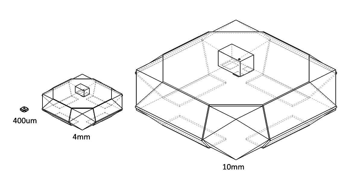
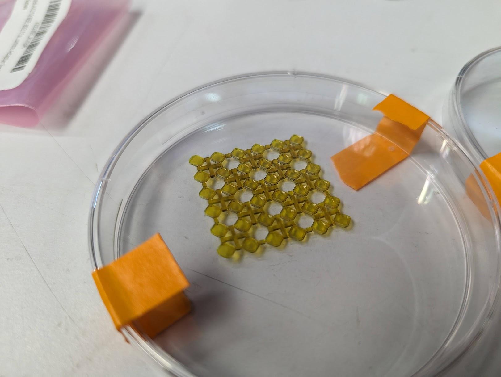
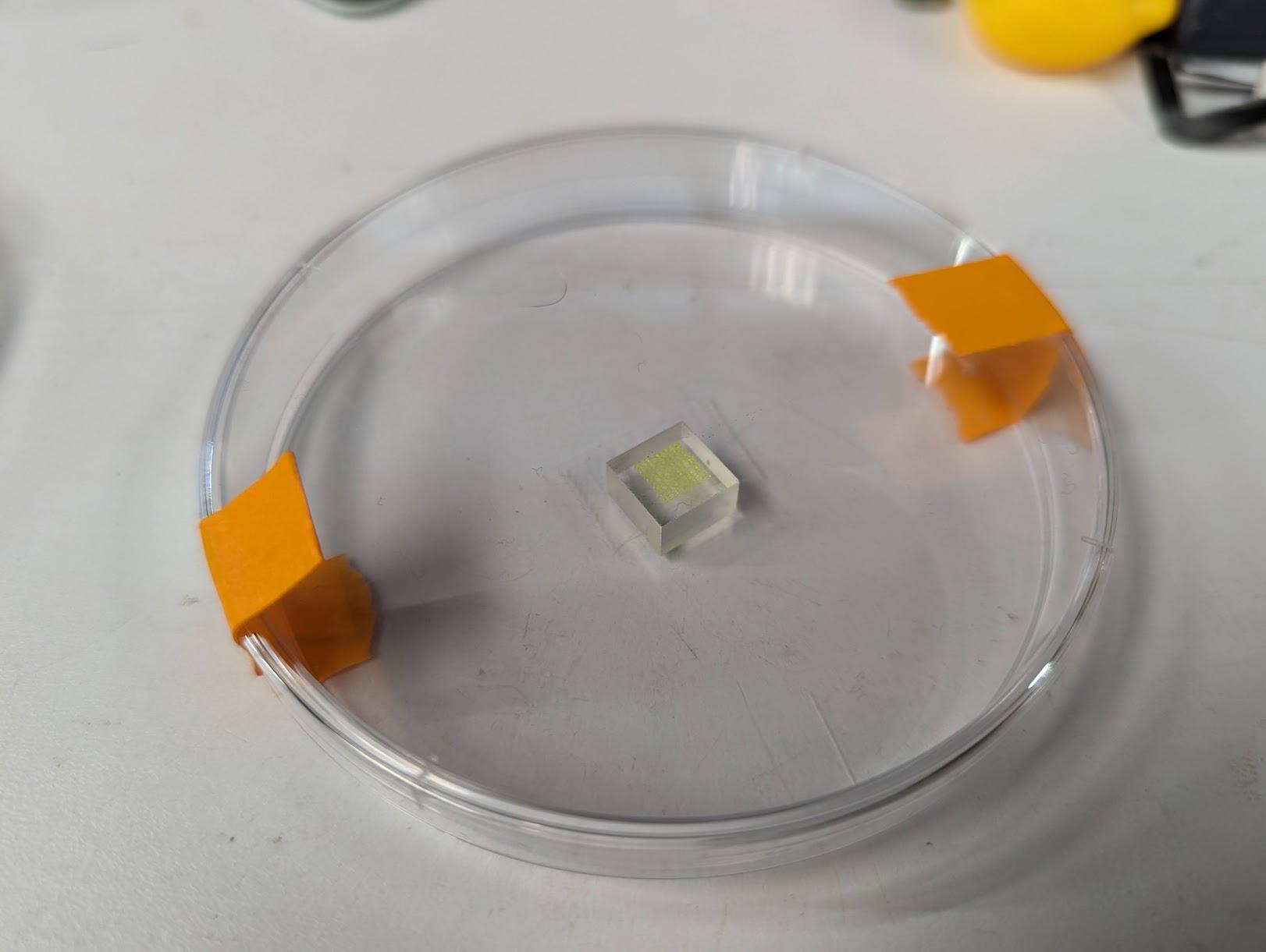

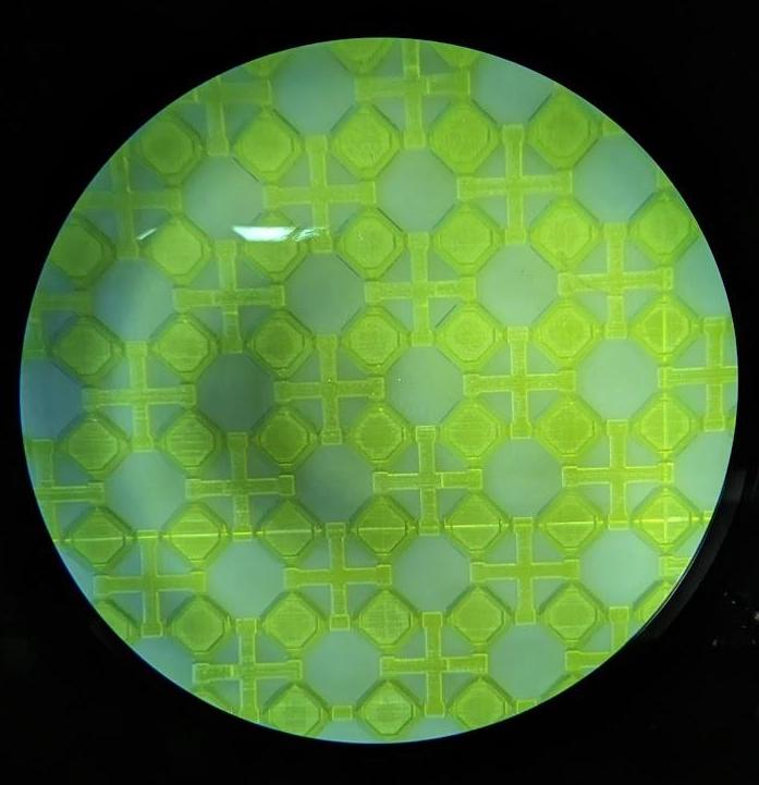
This miniaturization approach shifts the VMD paradigm closer to electronics packaging level 1 (device-in-IC) rather than level 2 (SMD-on-PCB). Beyond the obvious performance advantages from reduced parasitic effects, this scale reduction offers practical assembly benefits. Smaller elements enable more compact circuits, making parallel processing with multiple assembly machines more feasible by reducing the physical workspace requirements for complex structures.
6.1.6 Mini-Assembly Farms for Smaller Elements
Improving serial performance vs building parallel machines was discussed in Chapter 3. However, another interesting angle borrows from the abstraction levels introduced earlier for digital materials: what is the minimal form of a machine? My lab has been focused on this question for awhile, deriving inspiration from biology and working towards relative machines [9]; [10].
While the assemblers assembling assemblers arc is important this research space, it is fairly ambitious in the near term, and would be difficult to immediately apply to my geometry. A close analogy might be a minimal conventional machine that could be rapidly fabricated, assembled, and deployed. By reducing the complexity and footprint of individual assembly units, this approach could potentially enable higher density deployment of assembly capacity within a given workspace.
Critical to the success of assembly farms will be solving the challenges of machine-to-machine transport and registration. Effective systems must establish reliable protocols for transferring partially completed assemblies between machines while maintaining precise alignment. This would require advanced localization methods, potentially utilizing computer vision, fiducial markers, or mechanical registration features to ensure seamless coordination between independent assembly units working on different aspects or regions of a single construction.
The incremental improvements discussed earlier in the thesis combined with this more ambitious assembly farm concept provide a roadmap for scaling VMD assembly capacity by orders of magnitude beyond what has been demonstrated in this thesis.
6.1.7 Super-DICE 2.0
Super-DICE 2.0 picks up on Zach Fredin and Camron Blackburn’s work on Super-DICE [11] [12], this time working with Camron Blackburn and Alex Wynn; example devices from their work are shown in Figure 6.4.
Super conducting electronics (SCE) have unique packaging challenges. For one, Josephson Junctions (JJs), a fundamental building block for SCE, are fabricated at much coarser resolutions than conventional lithographic transistors, which makes it difficult to integrate sufficient complexity into a single die to enable compute applications (10k JJs vs millions, billions transistors). Modular approaches are therefore of great interest towards moving past single device performance.
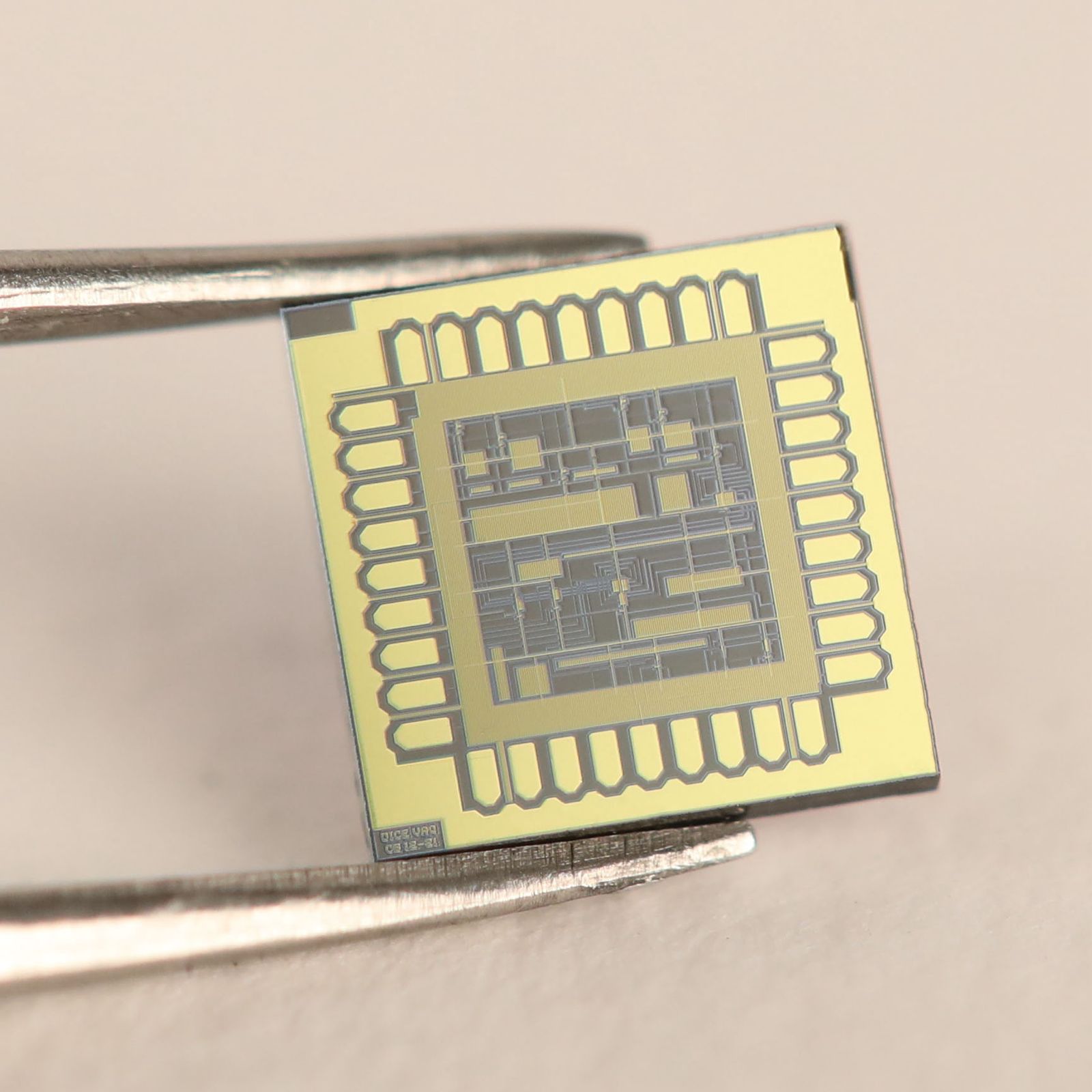
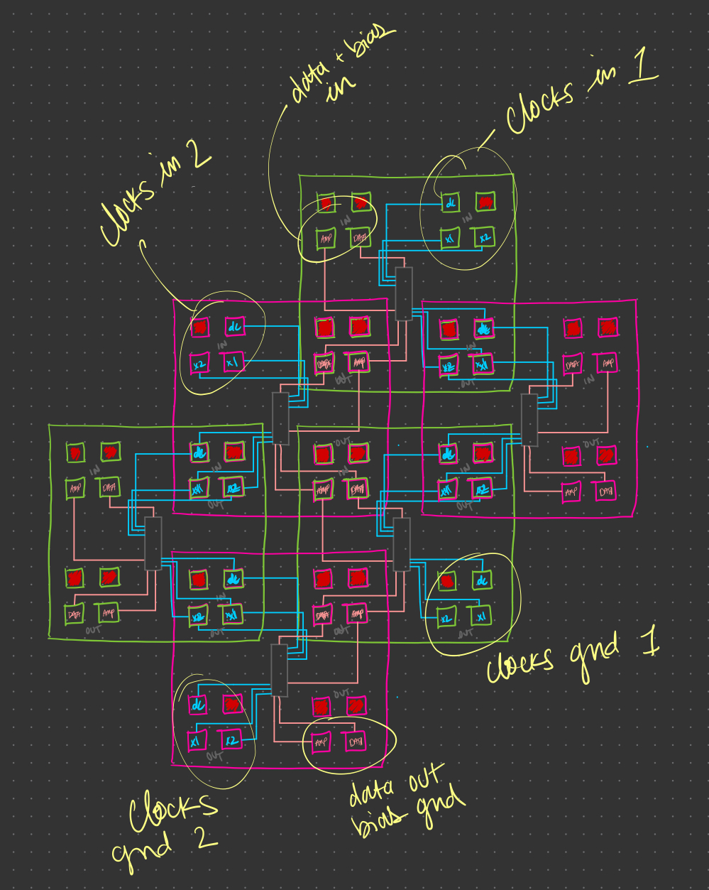
Using a modified 4BI approach, the plan is to assemble these devices. Devices will either be packaged onto PCB substrates as typical, or the bare die themselves can act as the tiles. This application is particularly interesting for 4BI, as it represents a major step towards the integrated device abstraction level, with higher i/o per interface (Figure 6.4 (b)).
6.2 Impact
The Volume Mount Device framework represents a fundamental reimagining of electronic systems integration, challenging the two-dimensional paradigm that has dominated the industry for decades. VMDs enable more resilient electronics that can withstand supply chain disruptions while opening design possibilities previously constrained by planar thinking. As the electronics industry pushes against the physical limits of traditional approaches, the volumetric integration methods demonstrated here offer a valuable complementary trajectory. Just as the transition to surface-mount technology revolutionized electronics manufacturing in the late 20th century, volume-mount devices may define the next generation of electronics integration.
the “C” in 4Cx could be interpretted as the shape of a compliant contact, in keeping with the naming scheme↩︎