Volume Mount Devices
1 Introduction
1.1 Motivation
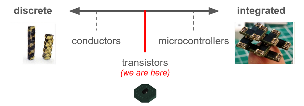
Moore’s law originated with Gordon Moore, who in 1965, observed that the number of transistors on an integrated circuit were doubling every two years. Later revised to every 1.5 years, Moore projected that transistors were on track to continue this trend for the next 10 years.
The practical implementation of Moore’s law was initially enabled by Dennard scaling, a principle formulated by Robert Dennard in 1974. Dennard scaling suggested that as transistors shrink, power density remains constant, allowing smaller transistors to operate at lower voltage, higher speeds, and with better power efficiency. This complementary principle meant that not only could more transistors fit on a chip (following Moore’s law), but they could also operate more efficiently, creating a self-sustaining cycle of performance improvement.
In fact, for the past 50+ years, Moore’s law has largely dominated the exponential performance increase seen by the computing industry, but due to the breakdown of Dennard scaling around 2006 [1] and physical limits, many have proclaimed Moore’s law dead [2]; [3]; [4]. Without Dennard scaling’s benefits, increased transistor density no longer automatically translates to proportional performance and efficiency gains. Transistors are still being improved [5], but no longer at the pace of Moore’s law, and with a higher price tag [6].
The end of Moore’s law has brought about demand for alternative solutions to continue increasing performance in lithography. This has placed a lot of focus on new approaches such as the Gate All Around FET (GAAFET) [7], back-side power delivery to alleviate on-device wiring density [8], and High-NA Extreme Ultra-Violet (EUV) lithography [9]; [10]; [11].
In particular, chiplets and heterogeneous integration (HI) [12]; [13] are a packaging innovation that enables designers to bring critical circuits closer together and fab designs on process nodes suitable for each chiplet, rather than compromising performance by using one node for the entire die, which can be challenging and expensive; power, compute, and MEMs all have different requirements, and different nodes are better for optimized for different applications.
While HI is now considered a mainstream advanced packaging technique that has allowed the industry to continue scaling performance, many of the viable implementations are still limited in the number of chiplets they can stack and interconnect; true 3d packaging without restriction is still out of reach, economically and technically. And while the semiconductor industry has access to HI, the rest of the electronics packaging stack has not been similarly improved, which reduces the effectiveness and accessibility of gains made in the semiconductor industry.
In this thesis, I focus on ground work developing the Volume Mount Device (VMD), a term initially coined by Ahmad Bahai and Neil Gershenfeld. This new packaging standard aims to eventually replace SMD and enable true 3d heterogeneous integration, refactoring the entire electronics stack instead of a small portion of it.
1.2 Electronics Packaging
Electronic packaging refers to the design and production of enclosures for electronic devices ranging from individual semiconductor devices up to complete systems. Packaging must address critical constraints including protection from mechanical damage, cooling, electromagnetic interference (EMI), and electrostatic discharge.
The conventional electronics packaging (EP) paradigm describes how electronics are physically packaged across multiple levels, from semiconductor devices to complete systems:
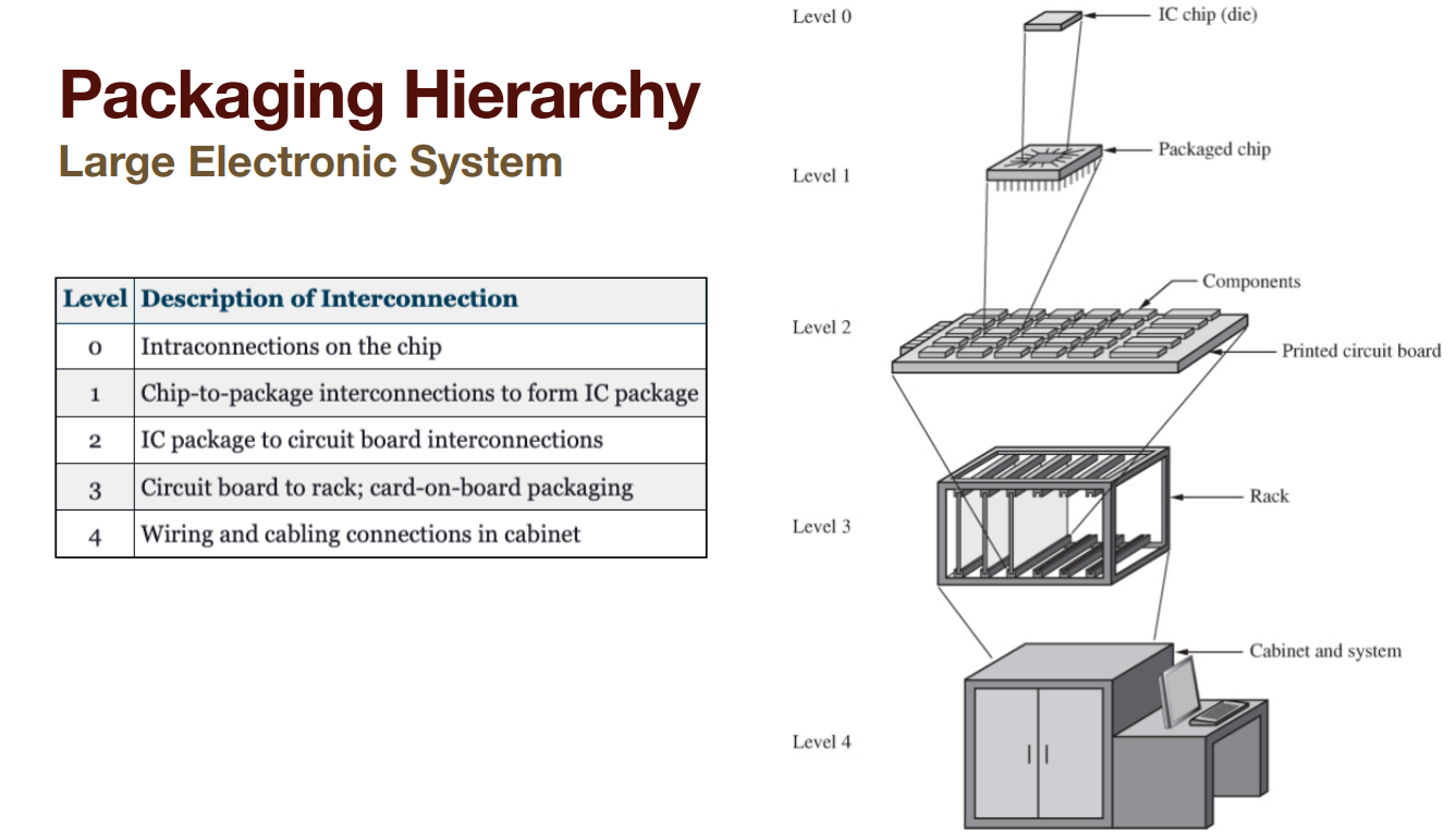
This EP structure describes the physical hierarchy of electronic systems, while the OSI model describes the digital communication hierarchy. Interconnects between these levels form their own hierarchy, often denoted as “half-levels” (0.5, 1.5, 2.5), representing the critical interfaces between major electronics packaging levels.
While this established EP hierarchy has enabled tremendous growth in computing capability, we’re now facing challenges with greater compute demands, power constraints, thermal limitations, and efficiency requirements. The semiconductor industry has responded with advanced packaging approaches, but these innovations have primarily focused on level 0 and 1, with limited transformation at higher levels.
1.2.1 Printed Circuit Boards
Printed circuit boards have evolved dramatically since Paul Eisler created the first true PCB in 1936 [14]. From simple single-layer boards to today’s complex high-density interconnect (HDI) PCBs with embedded components and 3D architectures, this technology has consistently improved to meet miniaturization and performance demands.
Despite these advances, multilayer PCBs remain accessible only at premium prices, and global supply chain disruptions (such as the COVID-19 pandemic [15] and trade tariffs [16]) have revealed significant vulnerabilities in this approach. And while a quick-turn PCB can be had in as little as a week, the centralized nature of manufacturing creates bottlenecks that can delay development by weeks or months. Decentralized means of PCB fabrication, such as cnc milled and laser ablated FR1 boards, are regularly used by fablabs, research institutions, and companies that need to quickly prototype, but these fabrication approaches usually don’t meet feature parity with ordered PCBs.
1.2.2 Integrated Circuit Packaging
IC packaging has similarly evolved from simple through-hole DIPs in the 1960s to today’s complex system-in-package designs. Surface-mount technology (SMT) became the dominant approach in the 1980s and 1990s, fundamentally changing electronics manufacturing while creating a standardized approach for component integration. And while SMT packages have progressively gotten smaller (BGAs and WLCSPs, 008004 and 006003 [17]; [18]), they’ve fundamentally remained the same as flat devices mounted to a flat substrate.
The biggest change to SMT has been occuring inside the package. Rather than relying solely on transistor scaling, HI focuses on integrating separately manufactured components into higher-level assemblies that provide enhanced functionality and improved operating characteristics. These assemblies are then typically still packaged as SMDs.
1.2.3 Heterogeneous Integration
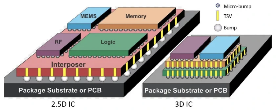
Heterogeneous integration represents the semiconductor industry’s embrace of modularity principles. By moving away from monolithic designs toward chiplet-based architectures, manufacturers can mix specialized components fabricated in different process nodes to optimize performance, reduce costs, and improve yields.
The evolution from 2.5D integration (lateral arrangement of chiplets on an interposer) [19]; [20]; [21] to 3D (vertical stacking) [22]; [23]; [24] and now 3.5D [25]; [26] approaches (combining both strategies) demonstrates the industry’s commitment to modularity as a path forward. Companies including AMD, Intel, TSMC, and Broadcom have pioneered commercial implementations of these technologies, with initiatives like Universal Chiplet Interconnect Express (UCIe) and Bunch of Wires (BoW) [27]; [28] attempting to standardize interfaces between components.
However, despite the performance gains made, heterogeneous integration approaches remain largely inaccessible to all but the most well-funded organizations due to several significant constraints.
HI technologies require advanced manufacturing capabilities exclusive to major semiconductor companies and foundries, while the specialized equipment, processes, and expertise involved impose prohibitive costs for smaller organizations. The integration of chiplets demands sophisticated thermal, mechanical, and electrical co-design capabilities that exceed what traditional EDA tools can provide [29]; [30]; [31], and the highly specialized nature of HI manufacturing introduces new supply chain vulnerabilities rather than mitigating existing ones. While proving to be a way forward, this concentration of capability limits innovation to a select few industry giants.
1.3 Supply Chain Challenges and Climate Implications
Electronics supply chain disruptions during COVID-19 created year-long lead times for integrated circuits critical to industries such as automotive and industrial manufacturing [15]. These shortages extended beyond ICs to materials like copper foil [32], impacting PCB production. Global trade tensions and tariffs have further exacerbated these vulnerabilities [16].
Despite government initiatives like the CHIPS Act [33]; [34]; [35] in the United States, robust solutions to supply chain resilience remain largely unimplemented. The centralized nature of electronics manufacturing creates fundamental vulnerabilities that legislation alone cannot address.
Furthermore, as computational demands grow (in particular with the surge in AI, large language models, and training infrastructure), the environmental impact of electronics manufacturing becomes increasingly significant [36]; [37]; [38]. Without more efficient approaches to electronics packaging and assembly, the climate impact of computing will likely worsen dramatically in coming years.
1.4 Accessible Modularity
Previous research in discretely assembled electronics has demonstrated potential for addressing both performance and supply chain challenges. Modular approaches have shown promise for both high-performance computing systems and lower-level electronics packaging, though physical implementations have typically been limited to tens of components rather than the hundreds or thousands needed for practical applications.
The challenge lies not only in technical feasibility but in creating solutions that remain accessible after implementation. Desktop-scale discrete electronics assembly offers a complementary approach to traditional manufacturing; not replacing it, but providing flexibility through localized assembly using standardized components sourced through diversified supply chains.
1.5 Related Work
1.5.1 Project Tinkertoy
The concept of modular electronic systems is not entirely new. In the 1950s, when PCBs already existed but most electronics were still manually assembled via labor-intensive methods like wire-wrapping [39]; [40], the U.S. National Bureau of Standards developed Project Tinkertoy [41], a pioneering modular electronics approach that used standardized ceramic wafers as building blocks for electronic circuits. These modules were designed to snap together to form functioning circuits, and although it was eventually superseded by PCBs and transistors, it played a large role in establishing the automation that drives those processes today.
1.5.2 Electronic Digital Materials
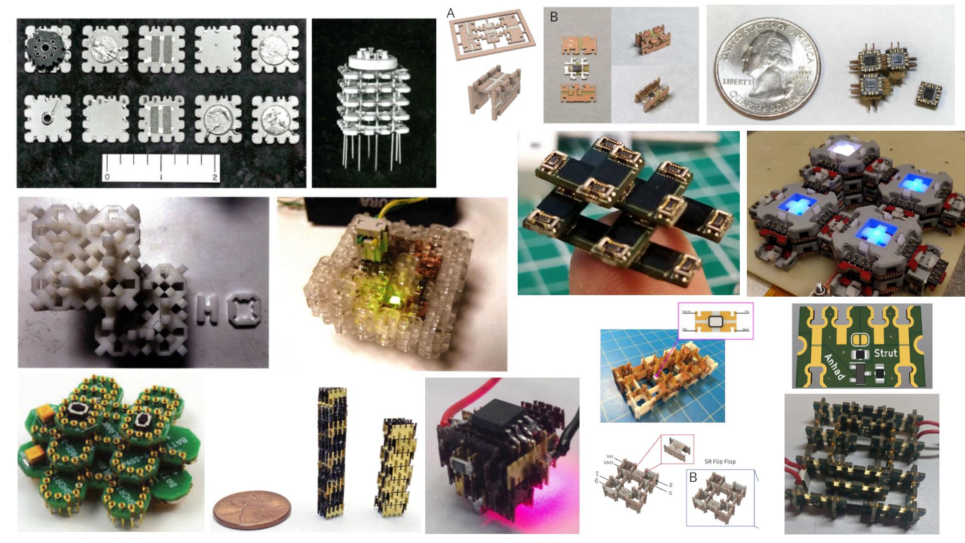
In the past two decades or so, more recent work has been done on electronic digital materials, a contemporary rebirth of the ideas that Project Tinkertoy put forth. These implementations have been explored from a variety of angles and abstraction levels by Fredin [42], Langford [43], Ward [44], MacCurdy [45], Hiller [46], and others.
These range from basic conductive and insulating elements, as demonstrated in Ward’s discretely assembled circuits and Langford’s GIK passive components, to component-level systems like BitBlox, to highly integrated programmable processor elements like DICE (Discrete Integrated Circuit Electronics).
These projects have demonstrated the fundamental feasibility of discretely assembled electronics but have generally been limited in assembly scale, automation capabilities, and practical applications. The VMD approach in subsequent chapters builds upon these foundations while addressing their limitations to create a truly scalable volumetric electronics paradigm.
Basic Bulk Materials
Ward [44], Langford [47], Hiller, and others have demonstrated basic electronic digital material systems of different geometries at various levels of automation.
In Jonathon Ward’s geometry [44], he demonstrates conductive and insulating assemblies up to 100 parts, manually assembled.
Additionally, in the process of building an LC resonator, Will Langford assembled an inductor from 520 parts via the time-honored fabrication process of GSWT (graduate students with tweezers, a manual process) [48].
Component Materials
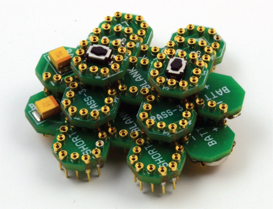
MacCurdy et al. Demonstrated the BitBlox platform with two significant implementations. The first was a two-channel infrared remote control constructed from 17 blocks representing 7 distinct functional types. This assembly was completed using an automated process, though no specific assembly time was documented [45]. In a more complex application, they created a five-channel infrared remote control utilizing 130 blocks across 7 functional types. This larger system was assembled manually and required approximately two hours for both design and assembly tasks [45]. These examples illustrate both the scalability of the BitBlox approach and the potential time efficiency advantages of automated assembly processes compared to manual construction for complex electronic systems. However, the paper also qualitatively suggested that the automated assembly process was only sometimes reliable.
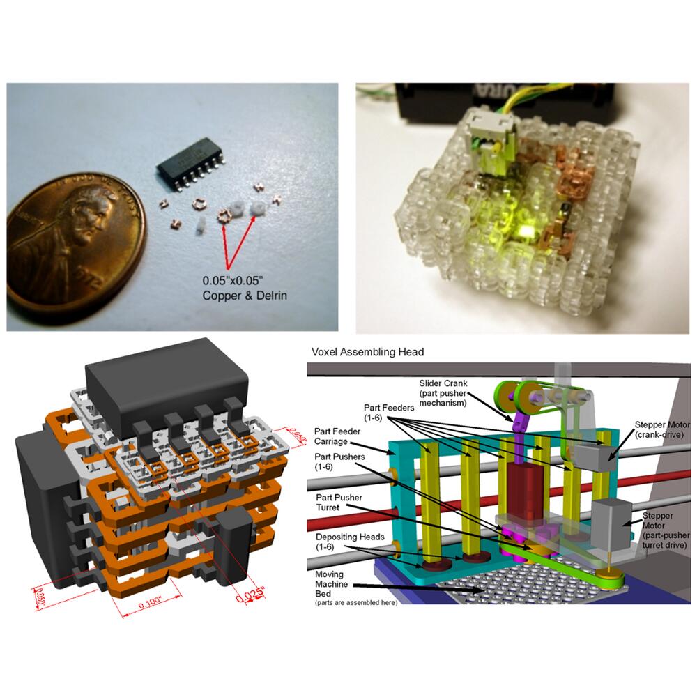
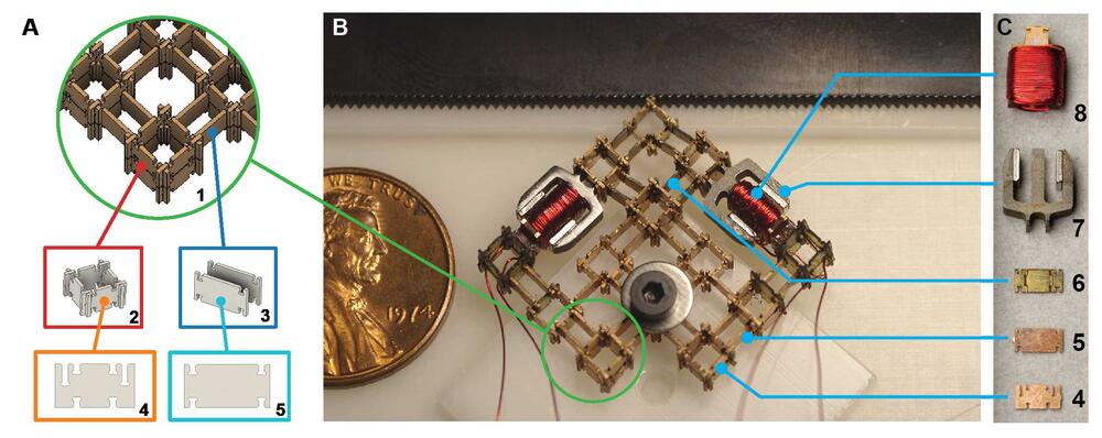
In his PhD thesis, Will also developed a robot assembler for automated assembly, which demonstrates constructing a walking motor from 20 nodes, 6 rigid struts, 4 flexural struts, and 2 actuators; in total, a 32-part walking motor in 8 minutes (4 parts/min, or 240 components per hour (CPH)) [47]. This system could handle 3 different element classes (nodes, struts, and actuators) via toolchanging, and incorporated many quality of life features, such as being able to change part-feeding magazines while jobs were running. However, the assembly rate is slow to build large complex assemblies within a reasonable amount of time; an entry-level desktop pick-and-place (PnP) is 1580 CPH, while this process is 240 CPH.
Discrete Integrated Circuit Electronics (DICE)
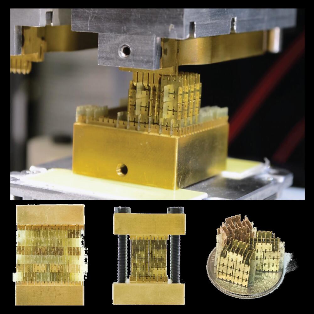
The term Discrete Integrated Circuit Electronics (DICE) was initially coined by Will Langford in his PhD thesis [47], and referred to an integrated electronic digital material design that relied on laminate layers to pack multiple conductive layers into an element.
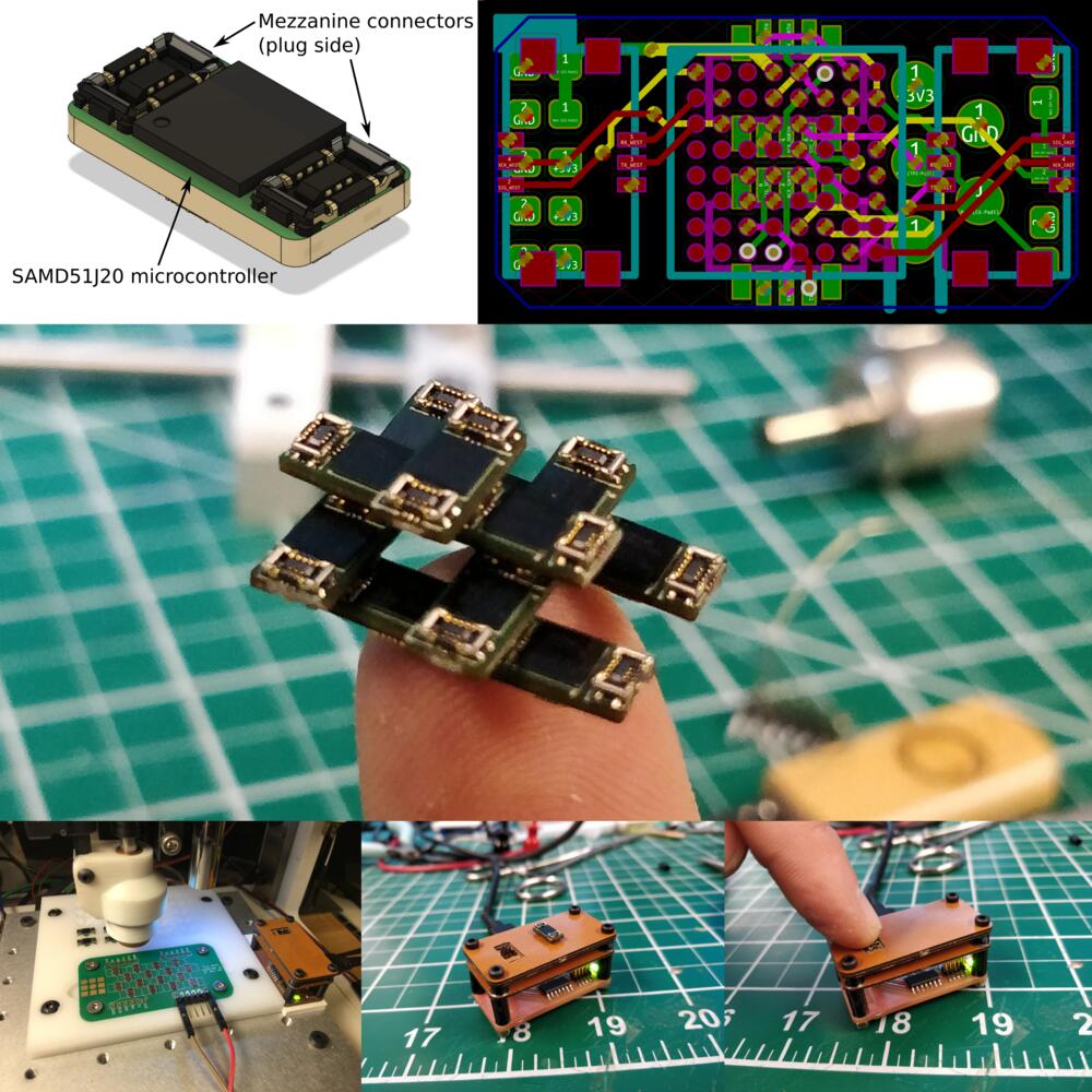
In Tiny-DICE, Zach Fredin designed and fabricated microcontroller assemblies using the smallest COTS components at the time; subcompact mezzanine connectors were used as interconnects for the elements, which were connected in a tetrahedral geometry [42].
His later iteration of Meso-DICE increased the size of the elements to explore more reliable interconnect mechanisms fabricated in-house, and prioritized reliability over feature size.
These geometries were built in 10s of elements, in Tiny-DICE’s case, it was a single type, and in Meso-DICE, it was 2 types.
In general, component and integrated level geometries share similar packaging challenges; to route multiple nets and build-in mechanical properties for alignment and retention, feature overhead must be added for reliable operation.
Abstraction Levels
The component abstraction level is the most flexible between basic and integrated, as it can be used for a variety of applications, including computational or power, and provide flexibility in how those applications are implemented. For example, computational architectures could be NMOS, CMOS, diode, etc. Additionally, the component abstraction level can expand to interoperate with basic and integrated abstraction levels easily through a compromise of design requirements; more basic elements can be incorporated by subdividing the component grid and reducing features, and more integrated elements with higher fan-out need only add ports by scaling up in the grid.
Comparatively, operating at the basic abstraction level requires a large amount of assembly to achieve a useful level of complexity; on the opposite end, operating at the processor level greatly reduces design flexibility to only include specific types of computational applications using the same computational architecture, and uses parts with higher overhead that makes it difficult to retool for different use cases.
1.6 Thesis Contributions and Overview
This thesis contributes a volumetrically scalable set of electronic building blocks that can be used to build architecturally agnostic computational logic at the component abstraction level, along with an assembly system for constructing sophisticated electronic circuits. Because the component abstraction level is inherently flexible, this system can be repurposed across multiple abstraction levels, from individual logic gates to integrated structures like operational amplifiers and processor cores.
In Chapter 2, I present a systematic exploration of VMD geometries, analyzing the critical design decisions that govern their effectiveness. I examine manufacturability constraints, electrical and mechanical performance requirements, and feature considerations that influenced the development process. This chapter introduces several candidate geometries, from the initial 4H family to the more refined 4B and 4BI implementations, documenting how each iteration addressed limitations in previous designs. I detail how different tile and connector designs affect mechanical stability, electrical performance, and automated assembly capability, establishing the foundation for a viable VMD ecosystem.
Chapter 3 details the circuit assembly system I developed to construct VMD-based circuits at scale. This chapter examines the motion system architecture, specialized feeders for component storage, substrate design for precise positioning, and end effector configurations optimized for reliable manipulation. I present assembly benchmarks that demonstrate the system’s progression from handling tens of components to reliably placing hundreds of elements with minimal human intervention. This chapter also analyzes potential fault states and error correction strategies critical for scaling to larger assemblies, representing a significant advancement beyond previous work in modular electronics.
Chapter 4 evaluates the performance characteristics of assembled VMD circuits, focusing on two critical aspects: joint reliability and electrical performance. I present analysis of normal force windows and resistance measurements for different contact implementations. The chapter also showcases some example applications through ring oscillator and logic gate implementations. Performance characterization extends to first-principles projections for scaled-down micro-regime implementations, establishing the performance envelope for future VMD development.
Chapter 5 examines the current and upcoming VMD fabrication processes, with particular focus on the development of the 4BIc geometry. This chapter details my process for rapidly prototyping electrical “Connectors in a Day” (eCiD) using commercially available digital fabrication tools, and documenting the challenges and solutions encountered when developing self-aligning connector interfaces that enhance reliability while maintaining accessibility.
Finally, Chapter 6 concludes with a synthesis of the research findings and outlines promising directions for future work, including potential applications in heterogeneous computing systems, superconducting electronics, and scaled-down implementations approaching the semiconductor integration level. This chapter positions VMDs within the broader context of electronics manufacturing evolution and discusses their potential impact on supply chain resilience and sustainable electronics development.
Collectively, these chapters document the development pathway from conceptual design to practical implementation, and aim to establish VMDs as a viable path towards truly volumetric electronics that bridges the gap between conventional packaging technologies and advanced heterogeneous integration techniques.